RM0440 Rev 4 139/2126
RM0440 Embedded Flash memory (FLASH) for category 3 devices
228
3.7.10 Flash PCROP1 End address register (FLASH_PCROP1ER)
Address offset: 0x28
Reset value: 0xX000 XXXX. Register bits are loaded with values from Flash memory at
OBL.
Access: no wait state when no Flash memory operation is on going, word, half-word access.
PCROP_RDP bit can be accessed with byte access.
Bits 31:15 Reserved, must be kept cleared
Bits 14:0 PCROP1_STRT: PCROP area start offset
DBANK=1
PCROP1_STRT contains the first double-word of the PCROP area for bank1.
DBANK=0
PCROP1_STRT contains the first 2xdouble-word of the PCROP area for all
memory.
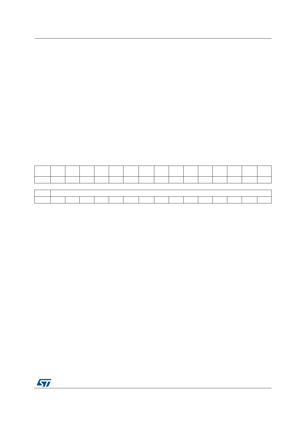
31 30 29 28 27 26 25 24 23 22 21 20 19 18 17 16
PCROP
_RDP
Res. Res. Res. Res. Res. Res. Res. Res. Res. Res. Res. Res. Res. Res. Res.
rs
15 14 13 12 11 10 9 8 7 6 5 4 3 2 1 0
Res. PCROP1_END[14:0]
rw rw rw rw rw rw rw rw rw rw rw rw rw rw rw
Bit 31 PCROP_RDP: PCROP area preserved when RDP level decreased
This bit is set only. It is reset after a full mass erase due to a change of RDP
from Level 1 to Level 0.
0: PCROP area is not erased when the RDP level is decreased from Level 1 to
Level 0.
1: PCROP area is erased when the RDP level is decreased from Level 1 to
Level 0 (full mass erase).
Bits 30:15 Reserved, must be kept cleared
Bits 14:0 PCROP1_END: Bank 1 PCROP area end offset
DBANK=1
PCROP1_END contains the last double-word of the bank 1 PCROP area.
DBANK=0
PCROP1_END contains the last 2x double-word of the first PCROP area in all
memory.
 Loading...


