RM0440 Rev 4 673/2126
RM0440 Analog-to-digital converters (ADC)
724
conversion if the complementary ADC is still sampling its input (only one ADC can sample
the input signal at a given time).
• The minimum possible DELAY is 1 to ensure that there is at least one cycle time
between the opening of the analog switch of the master ADC sampling phase and the
closing of the analog switch of the slave ADC sampling phase.
• The maximum DELAY is equal to the number of cycles corresponding to the selected
resolution. However the user must properly calculate this delay to ensure that an ADC
does not start a conversion while the other ADC is still sampling its input.
If the CONT bit is set on both master and slave ADCs, the selected regular channels of both
ADCs are continuously converted.
The software is notified by interrupts when it can read the data at the end of each
conversion event (EOC) on the slave ADC. A slave and master EOC interrupts are
generated (if EOCIE is enabled) and the software can read the ADC_DR of the slave/master
ADC.
Note: It is possible to enable only the EOC interrupt of the slave and read the common data
register (ADCx_CDR). But in this case, the user must ensure that the duration of the
conversions are compatible to ensure that inside the sequence, a master conversion is
always followed by a slave conversion before a new master conversion restarts. It is
recommended to use the MDMA mode.
It is also possible to have the regular data transferred by DMA. In this case, individual DMA
requests on each ADC cannot be used and it is mandatory to use the MDMA mode, as
following:
• Configure MDMA[1:0]=0b10 or 0b11 (depending on resolution).
• A single DMA channel is used (the one of the master). Configure the DMA master ADC
channel to read the common ADC register (ADCx_CDR).
• A single DMA request is generated each time both master and slave EOC events have
occurred. At that time, the slave ADC converted data is available in the upper half-word
of the ADCx_CDR 32-bit register and the master ADC converted data is available in the
lower half-word of ADCx_CCR register.
• Both EOC flags are cleared when the DMA reads the ADCx_CCR register.
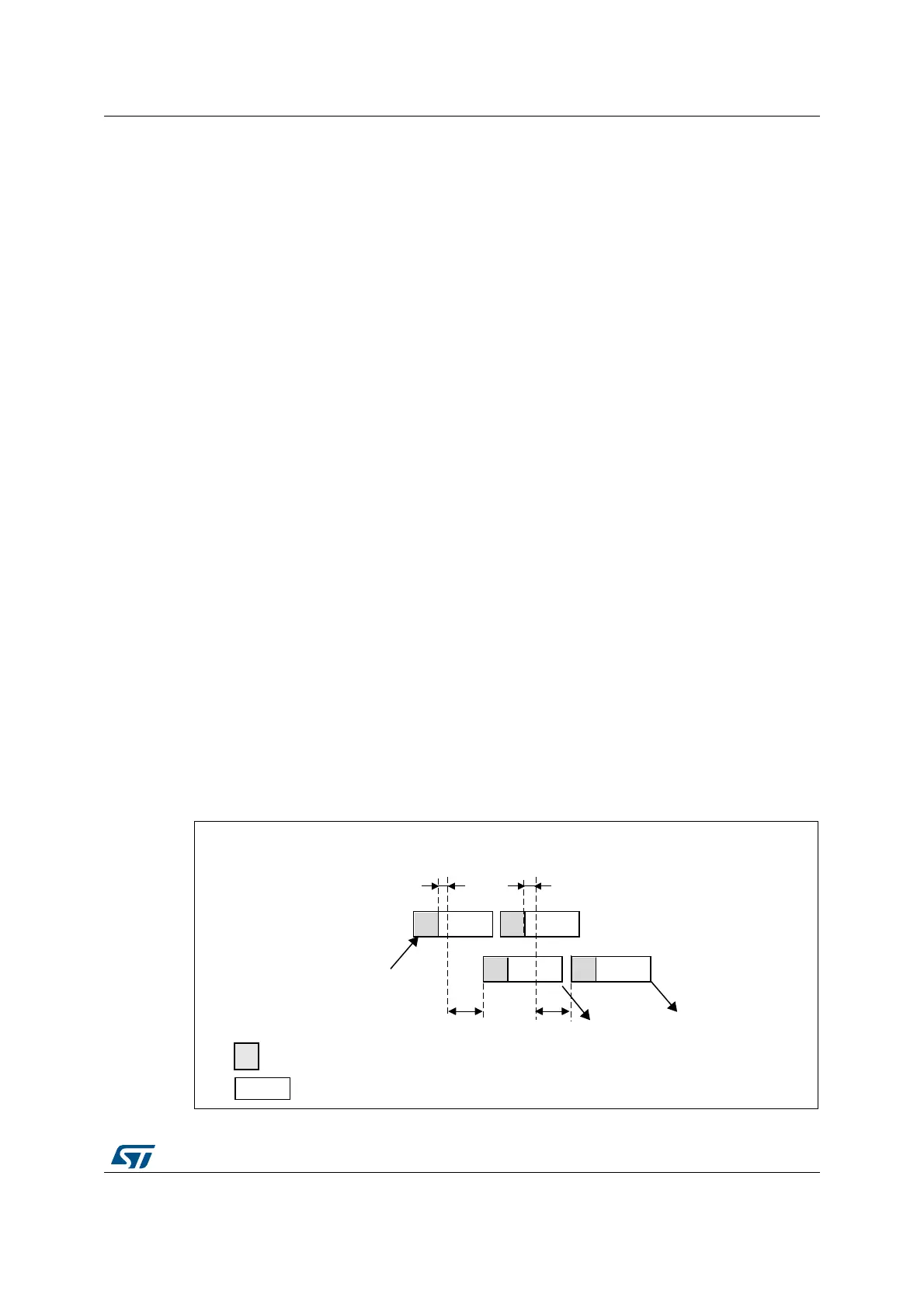
Figure 140. Interleaved mode on 1 channel in continuous conversion mode: dual ADC
mode
MSv31030V3
CH1
MASTER ADC
Trigger
Sampling
Conversion
4 ADCCLK
cycles
4 ADCCLK
cycles
SLAVE ADC
End of conversion on master and
slave ADC
0.5 ADCCLK
cycle
CH1
CH1
CH1
0.5 ADCCLK
cycle