RM0440 Rev 4 569/2126
RM0440 Flexible static memory controller (FSMC)
571
ECC result registers (FMC_ECCR)
Address offset: 0x94
Reset value: 0x0000 0000
This register contain the current error correction code value computed by the ECC
computation modules of the FMC NAND controller. When the CPU reads the data from a
NAND Flash memory page at the correct address (refer to Section 19.7.6: Computation of
the error correction code (ECC) in NAND Flash memory), the data read/written from/to the
NAND Flash memory are processed automatically by the ECC computation module. When
X bytes have been read (according to the ECCPS field in the FMC_PCR registers), the CPU
must read the computed ECC value from the FMC_ECC registers. It then verifies if these
computed parity data are the same as the parity value recorded in the spare area, to
determine whether a page is valid, and, to correct it otherwise. The FMC_ECCR register
should be cleared after being read by setting the ECCEN bit to 0. To compute a new data
block, the ECCEN bit must be set to 1.
Bits 7:0 ATTSET[7:0]: Attribute memory setup time
Defines the number of HCLK (+1) clock cycles to set up address before the command
assertion (NWE, NOE), for NAND Flash read or write access to attribute memory space on
socket:
0000 0000: 1 HCLK cycle
1111 1110: 255 HCLK cycles
1111 1111: reserved.
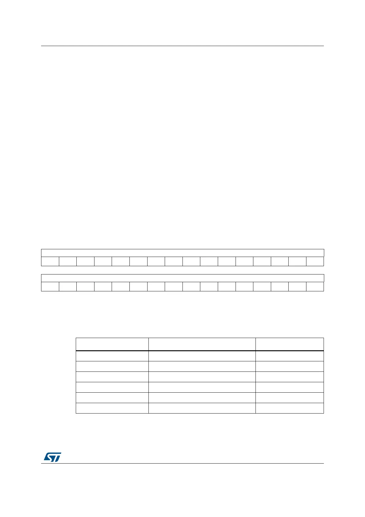
31 30 29 28 27 26 25 24 23 22 21 20 19 18 17 16
ECC[31:16]
rrrrrrrrrrrrrrrr
1514131211109876543210
ECC[15:0]
rrrrrrrrrrrrrrrr
Bits 31:0 ECC[31:0]: ECC result
This field contains the value computed by the ECC computation logic. Table 153 describes
the contents of these bitfields.
Table 153. ECC result relevant bits
ECCPS[2:0] Page size in bytes ECC bits
000 256 ECC[21:0]
001 512 ECC[23:0]
010 1024 ECC[25:0]
011 2048 ECC[27:0]
100 4096 ECC[29:0]
101 8192 ECC[31:0]
 Loading...


