Embedded Flash memory (FLASH) for category 3 devices RM0440
134/2126 RM0440 Rev 4
3.7.7 Flash ECC register (FLASH_ECCR)
Address offset: 0x18
Reset value: 0x0000 0000
Access: no wait state when no Flash memory operation is on going, word, half-word and
byte access
Bits 9:3 PNB[6:0]: Page number selection
These bits select the page to erase:
00000000: page 0
00000001: page 1
...
11111111: page 255
Bit 2 MER1: Bank 1 Mass erase
This bit triggers the bank 1 mass erase (all bank 1 user pages) when set.
Bit 1 PER: Page erase
0: page erase disabled
1: page erase enabled
Bit 0 PG: Programming
0: Flash programming disabled
1: Flash programming enabled
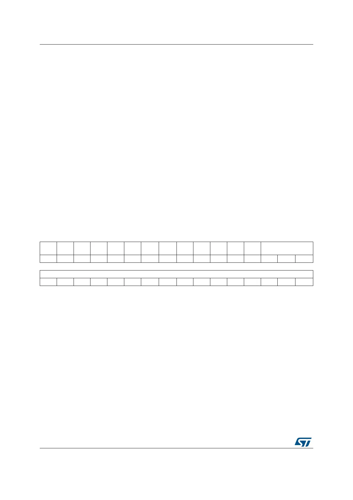
31 30 29 28 27 26 25 24 23 22 21 20 19 18 17 16
ECCD ECCC ECCD2 ECCC2 Res. Res. Res.
ECCC
IE
Res.
SYSF_
ECC
BK
_ECC
Res. Res. ADDR_ECC[18:16]
rc_w1 rc_w1 rc_w1 rc_w1 rw r r r r r
1514131211109 8 765432 1 0
ADDR_ECC[15:0]
rrrrrr r r rrrrrr r r
 Loading...


