RM0440 Rev 4 721/2126
RM0440 Analog-to-digital converters (ADC)
724
21.7.3 ADCx common regular data register for dual mode (ADCx_CDR)
(x=12 or 345)
Address offset: 0x0C (this offset address is relative to the master ADC base address +
0x300)
Reset value: 0x0000 0000
One interface controls ADC1 and ADC2, while the other interface controls ADC3, ADC4 and
ADC5.
21.8 ADC register map
The following table summarizes the ADC registers.
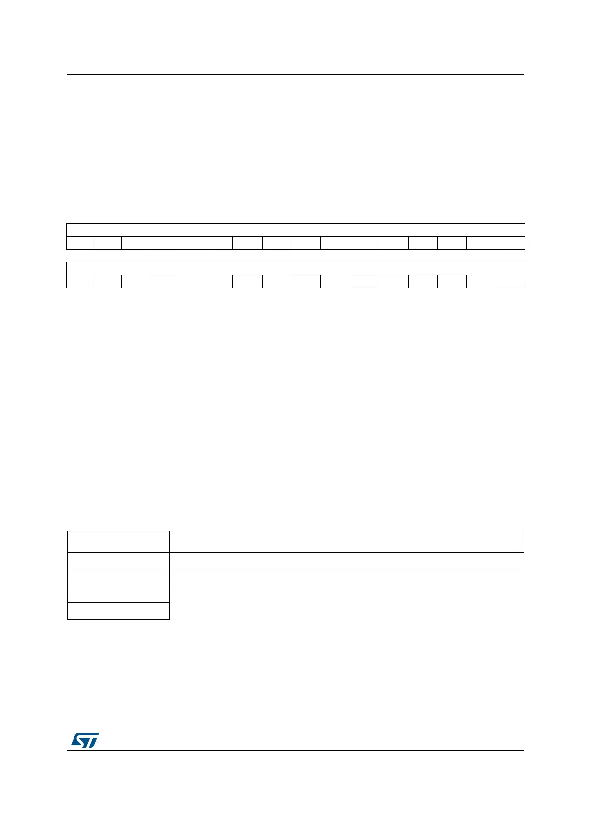
31 30 29 28 27 26 25 24 23 22 21 20 19 18 17 16
RDATA_SLV[15:0]
rrrrrr r r r r rrrrrr
1514131211109876543210
RDATA_MST[15:0]
rrrrrr r r r r rrrrrr
Bits 31:16 RDATA_SLV[15:0]: Regular data of the slave ADC
In dual mode, these bits contain the regular data of the slave ADC. Refer to Section 21.4.30:
Dual ADC modes.
The data alignment is applied as described in Section : Data register, data alignment and
offset (ADC_DR, OFFSETy, OFFSETy_CH, ALIGN))
Bits 15:0 RDATA_MST[15:0]: Regular data of the master ADC.
In dual mode, these bits contain the regular data of the master ADC. Refer to
Section 21.4.30: Dual ADC modes.
The data alignment is applied as described in Section : Data register, data alignment and
offset (ADC_DR, OFFSETy, OFFSETy_CH, ALIGN))
In MDMA=0b11 mode, bits 15:8 contains SLV_ADC_DR[7:0], bits 7:0 contains
MST_ADC_DR[7:0].
Table 176. ADC global register map
Offset Register
0x000 - 0x0FC Master ADC1/ADC3
0x100 - 0x1FC Slave ADC2/ADC4
0x200 - 0x2FC Reserved/single ADC5
0x300 - 0x30C Master and slave ADCs common registers
 Loading...


