Advanced-control timers (TIM1/TIM8/TIM20) RM0440
1128/2126 RM0440 Rev 4
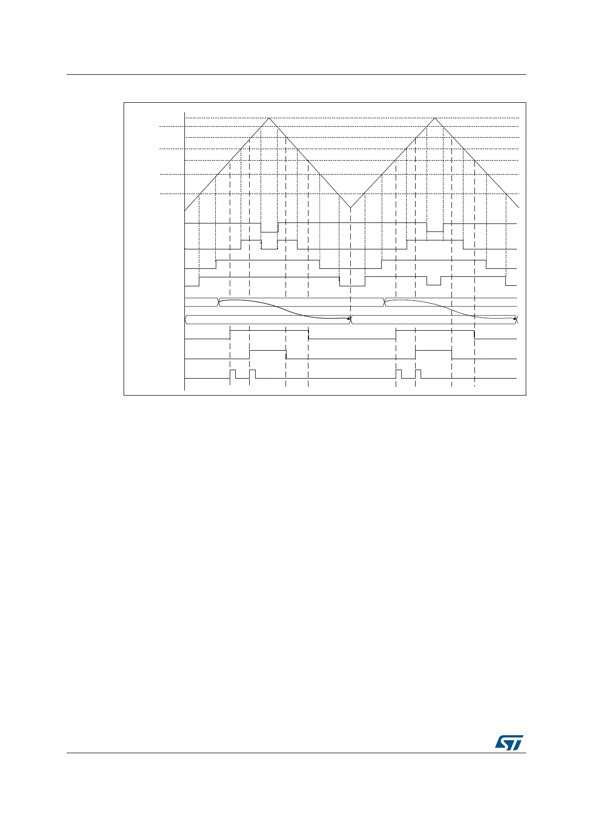
Figure 311. 3-phase combined PWM signals with multiple trigger pulses per period
The tim_trgo2 waveform shows how the ADC can be synchronized on given 3-phase PWM
signals. Please refer to Section 28.3.31: ADC synchronization for more details.
28.3.17 Complementary outputs and dead-time insertion
The advanced-control timers (TIM1/TIM8/TIM20) can output two complementary signals
and manage the switching-off and the switching-on instants of the outputs.
This time is generally known as dead-time and it has to be adjusted depending on the
devices that are connected to the outputs and their characteristics (intrinsic delays of level-
shifters, delays due to power switches...).
The polarity of the outputs (main output tim_ocx or complementary tim_ocxn) can be
selected independently for each output. This is done by writing to the CCxP and CCxNP bits
in the TIMx_CCER register.
The complementary signals tim_ocx and tim_ocxn are activated by a combination of several
control bits: the CCxE and CCxNE bits in the TIMx_CCER register and the MOE, OISx,
OISxN, OSSI and OSSR bits in the TIMx_BDTR and TIMx_CR2 registers. Refer to
Table 265: Output control bits for complementary tim_ocx and tim_ocxn channels with break
feature on page 1201 for more details. In particular, the dead-time is activated when
switching to the idle state (MOE falling down to 0).
Dead-time insertion is enabled by setting both CCxE and CCxNE bits, and the MOE bit if the
break circuit is present. There is one 10-bit dead-time generator for each channel. From a
MSv62331V1
ARR
CCR5
CCR1
CCR2
CCR3
tim_oc5ref
tim_oc1refc
CCR6
CCR4
100
xxx
001 100
Preload
GC5C[3:0]
xxx
Counter
tim_oc2refc
tim_oc3refc
Active
tim_oc4ref
tim_oc6ref
tim_trgo2
 Loading...


