Voltage reference buffer (VREFBUF) RM0440
774/2126 RM0440 Rev 4
23 Voltage reference buffer (VREFBUF)
23.1 Introduction
The devices embed a voltage reference buffer which can be used as voltage reference for
ADCs, DACs and also as voltage reference for external components through the VREF+
pin. When the VREF+ pin is double-bonded with VDDA pin in a package, the voltage
reference buffer is not available and must be kept disabled (refer to datasheet for packages
pinout description).
23.2 VREFBUF functional description
The internal voltage reference buffer supports three voltages
(a)
, which are configured with
VRS bits in the VREFBUF_CSR register:
• VRS = 00: around 2.048 V.
• VRS = 01: around 2.5 V.
• VRS = 10: around 2.90 V.
The internal voltage reference can be configured in four different modes depending on
ENVR and HIZ bits configuration. These modes are provided in the table below:
After enabling the VREFBUF by setting ENVR bit and clearing HIZ bit in the VREFBUF_CSR register,
the user must wait until VRR bit is set, meaning that the voltage reference output has reached its
expected value.
a. The minimum V
DDA
voltage depends on VRS setting, refer to the product datasheet.
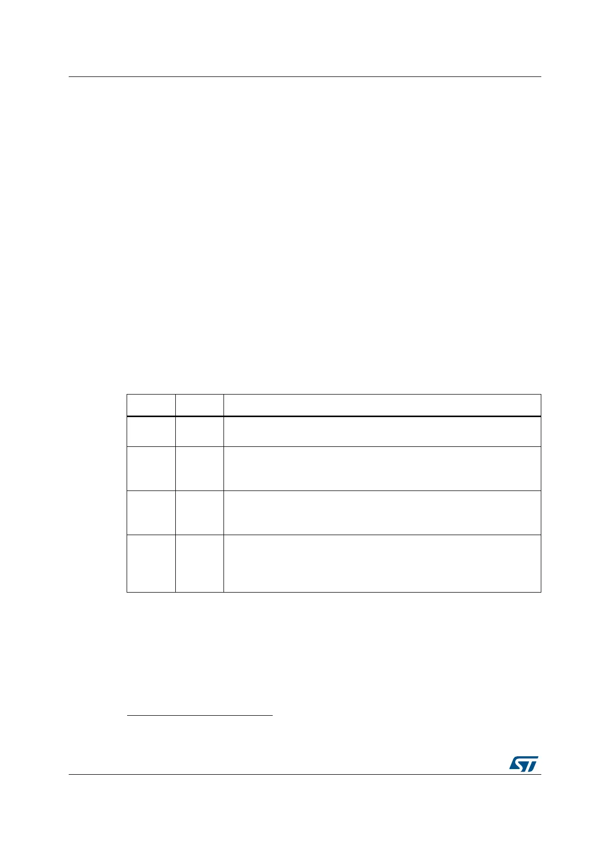
Table 193. VREF buffer modes
ENVR HIZ VREF buffer configuration
00
VREFBUF buffer off:
–V
REF+
pin pulled-down to V
SSA
01
External voltage reference mode (default value):
– VREFBUF buffer off
–V
REF+
pin input mode
10
Internal voltage reference mode:
– VREFBUF buffer ON
–V
REF+
pin connected to VREFBUF buffer output
11
Hold mode:
– VREFBUF buffer off
–V
REF+
pin floating. The voltage is held with the external capacitor
– VRR detection disabled and VRR bit keeps last state
 Loading...


