RM0440 Rev 4 1465/2126
RM0440 Low-power timer (LPTIM)
1487
32.3 LPTIM implementation
Table 309 describes LPTIM implementation on STM32G4 Series devices.
32.4 LPTIM functional description
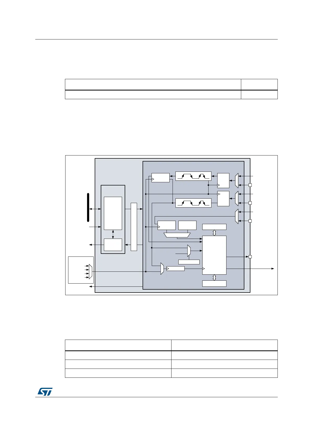
32.4.1 LPTIM block diagram
Figure 493. Low-power timer block diagram
1. lptim_out is the internal LPTIM output signal that can be connected to internal peripherals.
32.4.2 LPTIM input and trigger mapping
The LPTIM external trigger and input connections are detailed hereafter:
Table 309. STM32G4 Series LPTIM features
LPTIM modes/features
(1)
1. X = supported.
LPTIM1
Encoder mode X
MSv47458V2
LPTIM
Kernel clock domain
IRQ
interface
LPTIM
register
interface
APB clock
domain
32-bit APB bus
RCC
Wakeup
APB clock
LPTIM
interrupt
CLKMUX
16-bit counter
Count mode
16-bit compare
Prescaler
1
0
1
1
0
LPTIM_OUT
lptim_out
(1)
Synchronzation
HSI16
LSI
LSE
APB CLK
16-bit ARR
Mux trigger
Glitch
filter
CNTSTRT/
SNGSTRT
Glitch
filter
LPTIM_IN1
Encoder
Up/down
LPTIM_IN2
lptim_in2_1
lptim_in2_2
lptim_in2_3
lptim_in2_4
lptim_in1_1
lptim_in1_2
lptim_in1_3
lptim_in1_4
Glitch
filter
LPTIM_ETR
lptim_ext_trigx
Table 310. LPTIM1 external trigger connection
TRIGSEL External trigger
lptim_ext_trig0 GPIO
lptim_ext_trig1 RTC_ALARMA
lptim_ext_trig2 RTC_ALARMB
 Loading...


