Embedded Flash memory (FLASH) for category 4 devices RM0440
170/2126 RM0440 Rev 4
For example, to protect by WRP from the address 0x0801 2800 (included) to the address
0x0801 87FF (included):
• if boot in flash is selected, FLASH_WRP1AR register must be programmed with:
– WRP1A_STRT = 0x25.
– WRP1A_END = 0x30.
WRP1B_STRT and WRP1B_END in FLASH_WRP1BR can be used instead (area “B”
in Flash memory).
When WRP is active, it cannot be erased or programmed. Consequently, a software mass
erase cannot be performed if one area is write-protected.
If an erase/program operation to a write-protected part of the Flash memory is attempted,
the write protection error flag (WRPERR) is set in the FLASH_SR register. This flag is also
set for any write access to:
–OTP area
– part of the Flash memory that can never be written like the ICP
– PCROP area.
Note: When the memory read protection level is selected (RDP level = 1), it is not possible to
program or erase Flash memory if the CPU debug features are connected (JTAG or single
wire) or boot code is being executed from RAM or System flash, even if WRP is not
activated.
Note: To validate the WRP options, the option bytes must be reloaded through the OBL_LAUNCH
bit in Flash control register.
4.5.4 Securable memory area
The Securable memory area defines an area of code which can be executed only once at
boot, and never again unless a new reset occurs.
The main purpose of the Securable memory area is to protect a specific part of Flash
memory against undesired access. This allows implementing software security services
such as secure key storage or safe boot. Securable memory area is located in the Main
Flash memory. It is dedicated to executing trusted code. When not secured, the Securable
memory behaves like the remainder of Main Flash memory. When secured (the
SEC_PROT1 bit of the FLASH_CR register set), any attempt to program or erase in a
secure memory area generates a write protection error (WRPERR flag is set) and any
attempt to read from it generates a read error (RDERR flag is set).
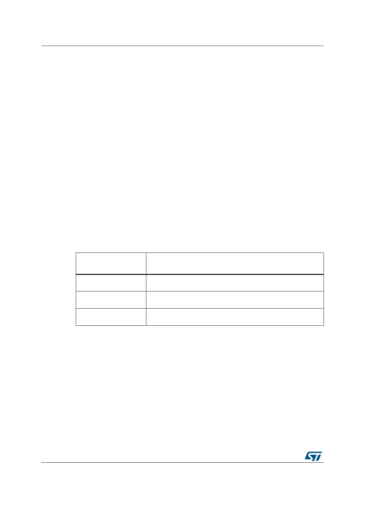
Table 25. WRP protection
WRP registers values
(x=1 y= A/B)
WRP protection area
WRPxy_STRT =
WRPxy_END
Page WRPxy is protected.
WRPxy_STRT >
WRPxy_END
No WRP area.
WRPxy_STRT <
WRPxy_END
The pages from
WRPxy_STRT to WRPxy_END are protected.
 Loading...


