RM0440 Rev 4 125/2126
RM0440 Embedded Flash memory (FLASH) for category 3 devices
228
If an erase/program operation to a write-protected part of the Flash memory is attempted,
the write protection error flag (WRPERR) is set in the FLASH_SR register. This flag is also
set for any write access to:
–OTP area
– part of the Flash memory that can never be written like the ICP
– PCROP area.
Note: When the memory read protection level is selected (RDP level = 1), it is not possible to
program or erase Flash memory if the CPU debug features are connected (JTAG or single
wire) or boot code is being executed from RAM or System flash, even if WRP is not
activated.
Note: To validate the WRP options, the option bytes must be reloaded through the OBL_LAUNCH
bit in Flash control register.
Note: When DBANK=0, it is the user’s responsibility to make sure that no overlapping occurs on
the WRP zone.
3.5.4 Securable memory area
The Securable memory area defines an area of code which can be executed only once at
boot, and never again unless a new reset occurs.
The main purpose of the Securable memory area is to protect a specific part of Flash
memory against undesired access. This is a mean to isolate first stage firmware boot
together with its sensitive assets (keys) from the rest of the application code. This allows
implementing root of trust solution such as secure boot. Securable memory area is located
in the Main Flash memory. It is dedicated to executing trusted code. When not secured, the
Securable memory behaves like the remainder of Main Flash memory. When secured (the
SEC_PROT1 (or SEC_PROT2) bit of the FLASH_CR register set), any attempt to program
or erase in a secure memory area generates a write protection error (WRPERR flag is set)
and any attempt to read from it generates a read error (RDERR flag is set).
The size of the Securable memory area is defined by the SEC_SIZE1[7:0] (or
SEC_SIZE2[7:0]) bitfield of the FLASH_SEC1R (or FLASH_SEC2R) register. It can be
modified only in RDP Level 0. Its content is erased upon changing from RDP Level 1 to
Level 0, even if it overlaps with PCROP pages.
3.5.5 Disabling core debug access
For executing sensitive code or manipulating sensitive data in Securable memory area, the
debug access to the core can temporarily be disabled.
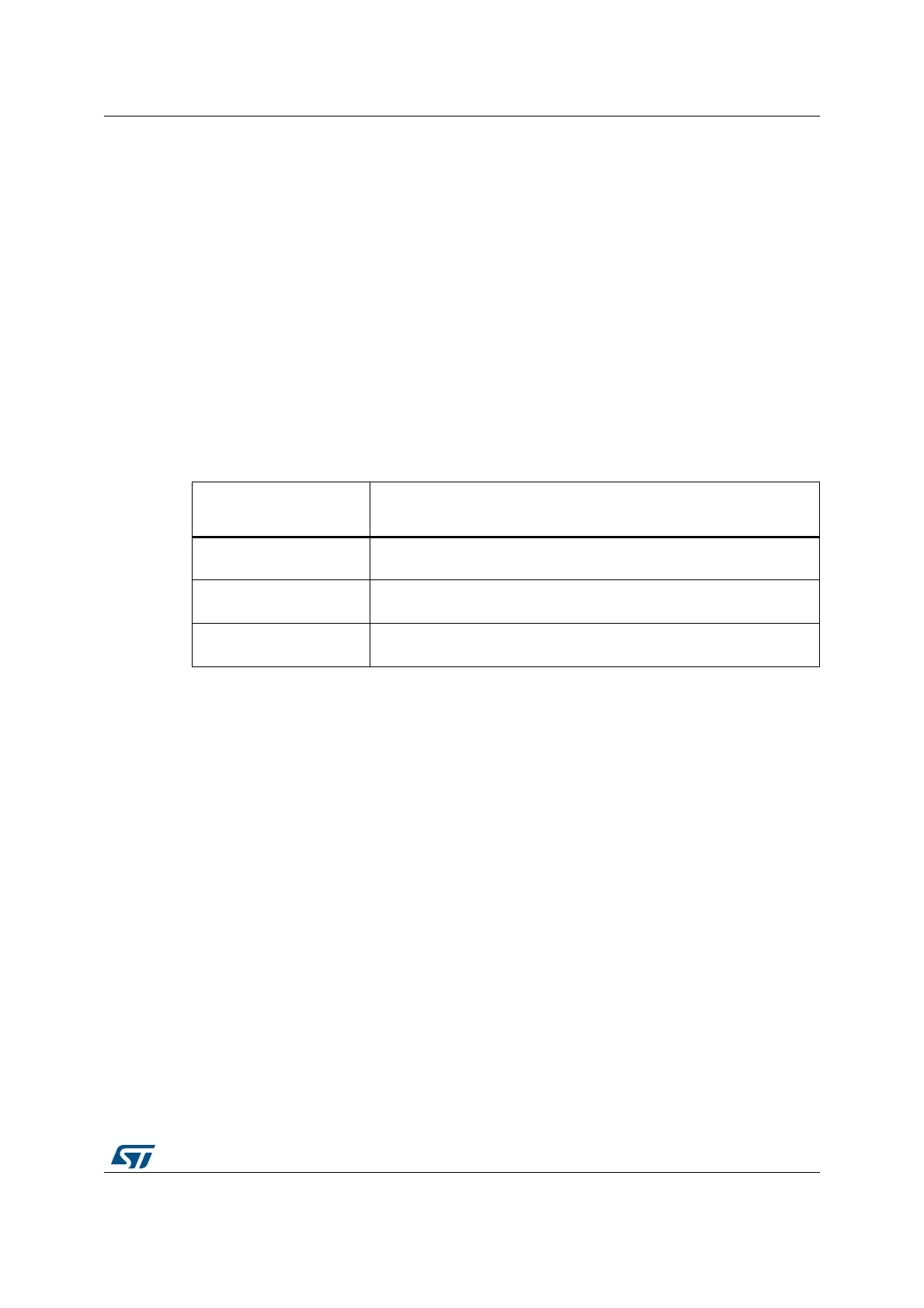
Table 15. WRP protection
WRP registers values
(x=1/2 y= A/B)
WRP protection area
WRPxy_STRT =
WRPxy_END
Page WRPxy is protected.
WRPxy_STRT >
WRPxy_END
No WRP area.
WRPxy_STRT <
WRPxy_END
The pages from
WRPxy_STRT to WRPxy_END are protected.
 Loading...


