Clock recovery system (CRS) RM0440
340/2126 RM0440 Rev 4
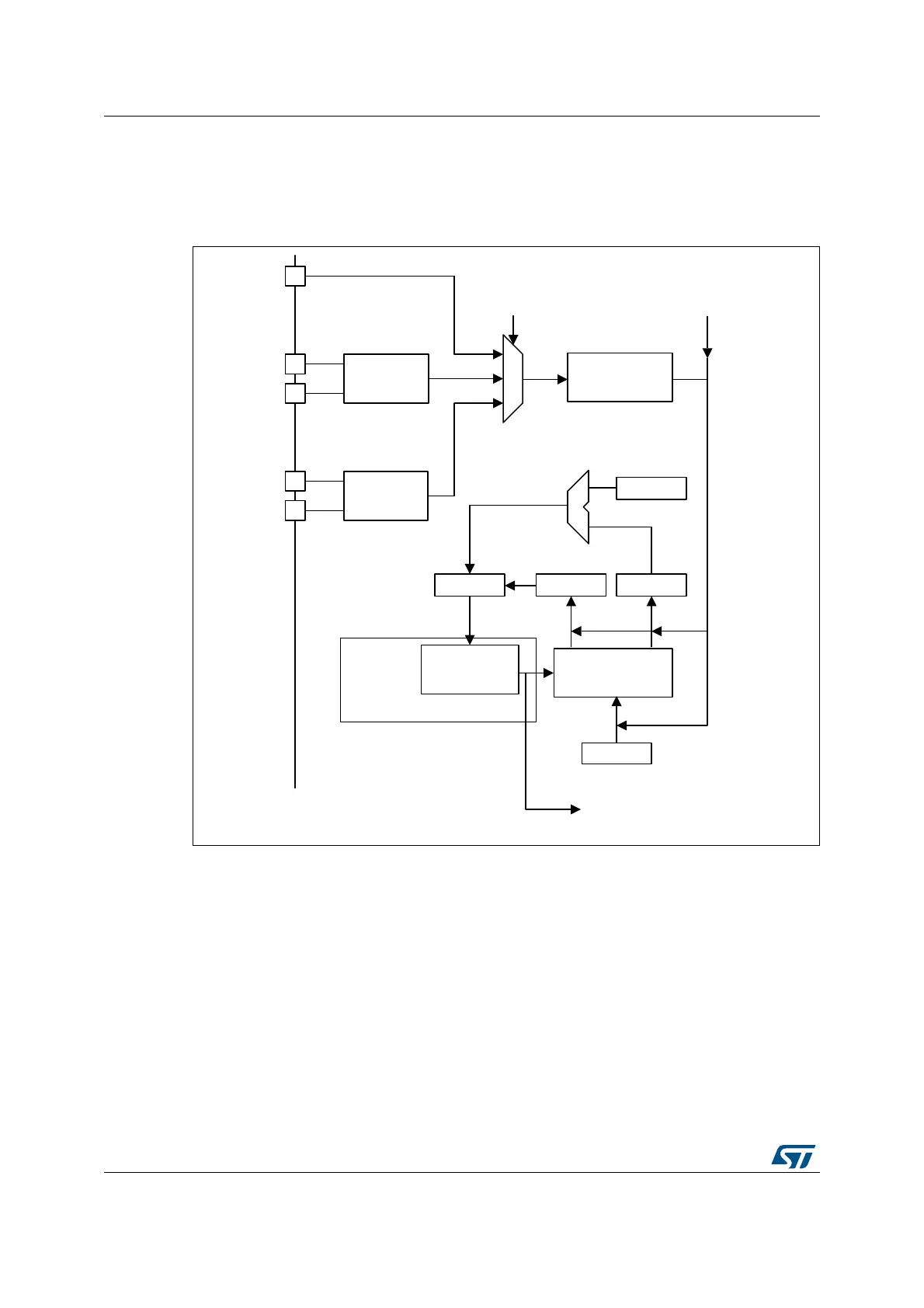
8.4 CRS functional description
8.4.1 CRS block diagram
Figure 23. CRS block diagram
8.4.2 Synchronization input
The CRS synchronization (SYNC) source, selectable through the CRS_CFGR register, can
be the signal from the LSE clock or the USB SOF signal. For a better robustness of the
SYNC input, a simple digital filter (2 out of 3 majority votes, sampled by the RC48 clock) is
implemented to filter out any glitches. This source signal also has a configurable polarity
and can then be divided by a programmable binary prescaler to obtain a synchronization
signal in a suitable frequency range (usually around 1 kHz).
For more information on the CRS synchronization source configuration, refer to
Section 8.7.2: CRS configuration register (CRS_CFGR).
It is also possible to generate a synchronization event by software, by setting the SWSYNC
bit in the CRS_CR register.
MSv34708V1
LSE
USB
SYNCSRC
GPIO
OSC32_IN
OSC32_OUT
USB_DP
USB_DM
SYNC divider
(/1,/2,/4,…,/128)
SWSYNC
RELOAD
SYNC
16-bit counter
FECAP
RC 48 MHz
HSI48
RCC
CRS_SYNC
FELIM
TRIM FEDIR
To USB
To RNG
 Loading...


