RM0440 Rev 4 165/2126
RM0440 Embedded Flash memory (FLASH) for category 4 devices
228
If the comparison between the word and its complement fails, a status bit OPTVERR is set.
Mismatch values are forced into the option registers:
– For USR OPT option, the value of mismatch is all options at ‘1’, except for
BOR_LEV which is “000” (lowest threshold)
– For WRP option, the value of mismatch is the default value “No protection”
– For RDP option, the value of mismatch is the default value “Level 1”
– For PCROP, the value of mismatch is “all memory protected”
On system reset rising, internal option registers are copied into option registers which can
be read and written by software (FLASH_OPTR, FLASH_PCROP1SR,
FLASH_PCROP1ER, FLASH_WRP1AR, FLASH_WRP1BR). These registers are also used
to modify options. If these registers are not modified by user, they reflects the options states
of the system. See Section : Modifying user options for more details.
4.5 FLASH memory protection
The Flash main memory can be protected against external accesses with the Read
protection (RDP). The pages of the Flash memory can also be protected against unwanted
write due to loss of program counter contexts. The write-protection (WRP) granularity is one
page (2 KByte). Apart of the flash memory can also be protected against read and write
from third parties (PCROP). The PCROP granularity is double word (64-bit).
4.5.1 Read protection (RDP)
The read protection is activated by setting the RDP option byte and then, by applying a
system reset to reload the new RDP option byte. The read protection protects to the Flash
main memory, the option bytes, the backup registers (RTC_BKPxR in the RTC) and the
CCM SRAM.
Note: If the read protection is set while the debugger is still connected through JTAG/SWD, apply
a POR (power-on reset) instead of a system reset.
There are three levels of read protection from no protection (level 0) to maximum protection
or no debug (level 2).
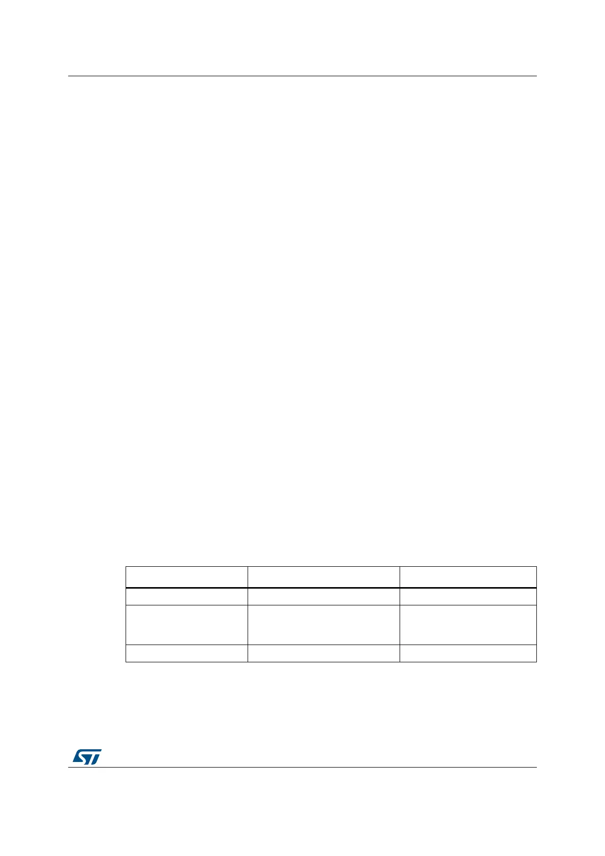
The Flash memory is protected when the RDP option byte and its complement contain the
pair of values shown in Table 32.
The System memory area is read accessible whatever the protection level. It is never
accessible for program/erase operation.
Table 22. Flash memory read protection status
RDP byte value RDP complement value Read protection level
0xAA 0x55 Level 0
Any value except 0xAA or
0xCC
Any value (not necessarily
complementary) except 0x55 and
0x33
Level 1 (default)
0xCC 0x33 Level 2
 Loading...


