RM0440 Rev 4 189/2126
RM0440 Embedded Flash memory (FLASH) for category 2 devices
228
5.3 FLASH functional description
5.3.1 Flash memory organization
The Flash memory has the following main features:
• Capacity up to 128 Kbytes (read width of 64-bits)
• 128 KB organized in one single bank for main memory
• Page size of 2 Kbyte
• 72 bits wide data read (64 bits plus 8 ECC bits)
• Page and Mass erase
• Each page is composed of 8 rows of 256 bytes
• An Information block containing:
– System memory from which the device boots in System memory boot mode. The
area is reserved for use by STMicroelectronics and contains the boot loader that is
used to reprogram the Flash memory through one of the following interfaces:
USART, SPI, I2C, USB. It is programmed by STMicroelectronics when the device
is manufactured, and protected against spurious write/erase operations. For
further details, please refer to the AN2606 available from www.st.com.
– 1 Kbyte (128 double word) OTP (one-time programmable) bytes for user data. The
OTP data cannot be erased and can be written only once. If only one bit is at 0,
the entire double word cannot be written anymore, even with the value 0x0000
0000 0000 0000.
– Option bytes for user configuration.
The memory organization is based on a main area and an information block as shown in
Table 28.
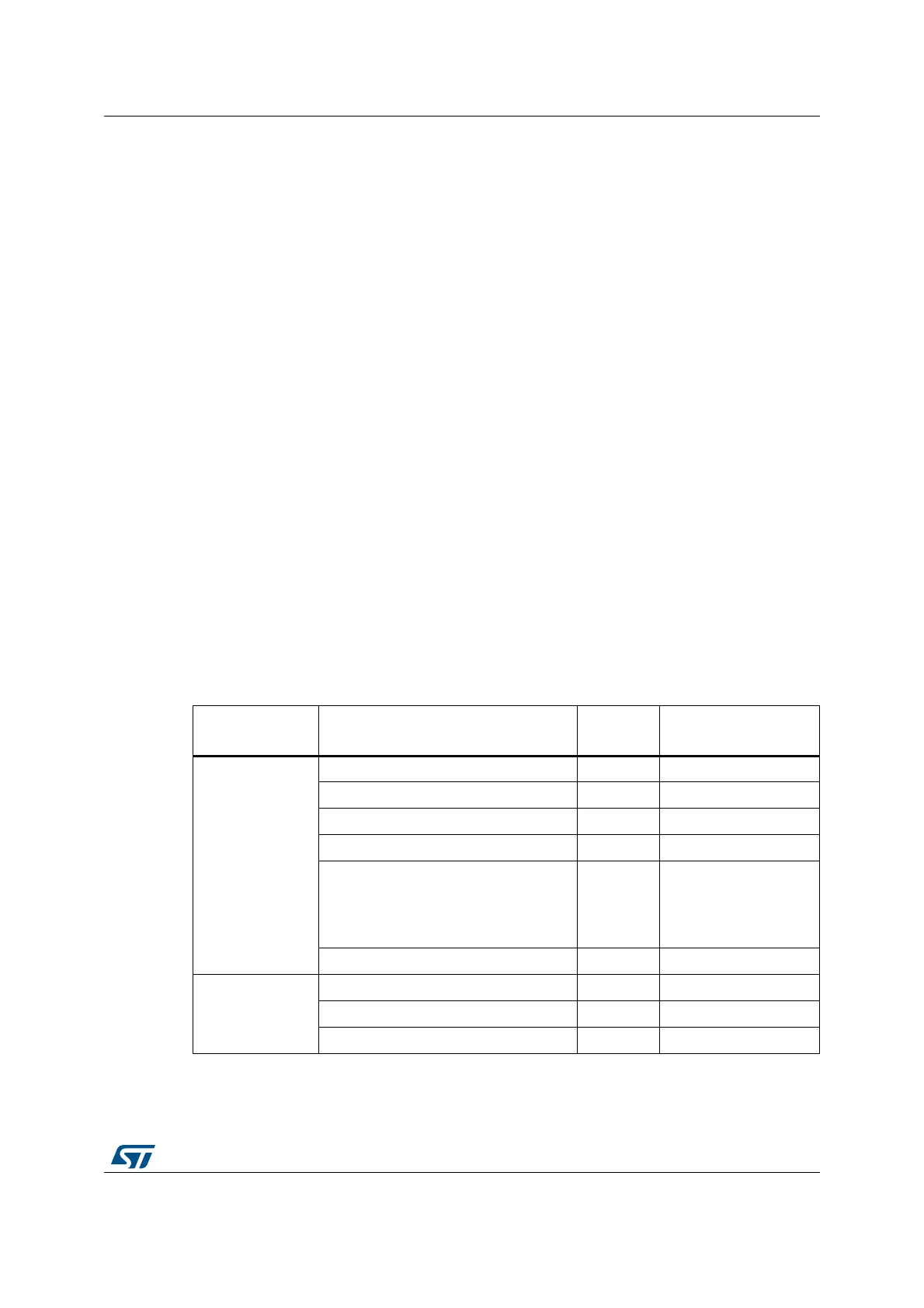
Table 28. Flash module organization (64 bits read width)
Flash area Flash memory addresses
Size
(bytes)
Name
Main memory
0x0800 0000 - 0x0800 07FF 2 K Page 0
0x0800 0800 - 0x0800 0FFF 2 K Page 1
0x0800 1000 - 0x0800 17FF 2 K Page 2
0x0800 1800 - 0x0800 1FFF 2 K Page 3
-
-
-
-
-
-
-
-
-
-
-
-
0x0801 F800 - 0x0801 FFFF 2 K Page 63
Information block
0x1FFF 0000 - 0x1FFF 6FFF 28 K System memory
0x1FFF 7000 - 0x1FFF 73FF 1 K OTP area
0x1FFF 7800 - 0x1FFF 782F 48 Option bytes
 Loading...


