Digital-to-analog converter (DAC) RM0440
736/2126 RM0440 Rev 4
22.4.5 DAC conversion
The DAC_DORx cannot be written directly and any data transfer to the DAC channelx must
be performed by loading the DAC_DHRx register (write operation to DAC_DHR8Rx,
DAC_DHR12Lx, DAC_DHR12Rx, DAC_DHR8RD, DAC_DHR12RD or DAC_DHR12LD).
Data stored in the DAC_DHRx register are automatically transferred to the DAC_DORx
register after one dac_hclk clock cycle, if no hardware trigger is selected (TENx bit in
DAC_CR register is reset). However, when a hardware trigger is selected (TENx bit in
DAC_CR register is set) and a trigger occurs, the transfer is performed three dac_hclk clock
cycles after the trigger signal.
When DAC_DORx is loaded with the DAC_DHRx contents, the analog output voltage
becomes available after a time t
SETTLING
that depends on the power supply voltage and the
analog output load.
HFSEL bits of DAC_MCR must be set when dac_hclk clock speed is faster than 80 MHz. It
adds an extra delay to the transfer from DAC_DHRx register to DAC_DORx register.
Refer to Table HFSEL description below for the limitation of the DAC_DORx update rate
depending on HFSEL bits and dac_hclk clock frequency.
If the data is updated or a software/hardware trigger event occurs during the non-allowed
period, the peripheral behavior is unpredictable.
The above timing is only related to the limitation of the DAC interface. Refer also to the
t
SETTLING
parameter value in the product datasheet.
1 0x000 0x800
1 0xFFF 0x7FF
1 0x800 0x000
Table 186. Data format (case of 12-bit data) (continued)
SINFORMATx bit
DATA written to DHRx
register
DATA transfered to DORx register
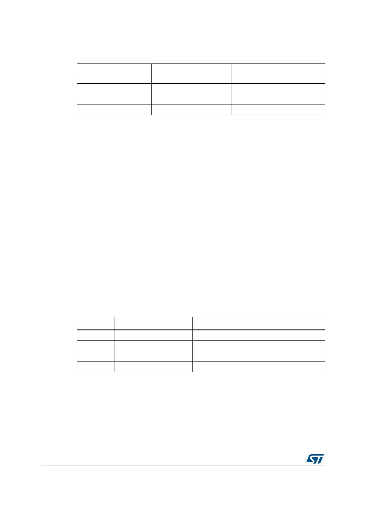
Table 187. HFSEL description
HFSEL[1:0] AHB frequency Function
00 ≤ 80 MHz DAC_DOR update rate up to 3 AHB clock cycles
01 >80 MHz
(1)
1. Refer to the device datasheet for the value of the maximum AHB frequency.
DAC_DOR update rate up to 5 AHB clock cycles
10 >160 MHz DAC_DOR update rate up to 7 AHB clock cycles
11 Reserved -
 Loading...


