Quad-SPI interface (QUADSPI) RM0440
574/2126 RM0440 Rev 4
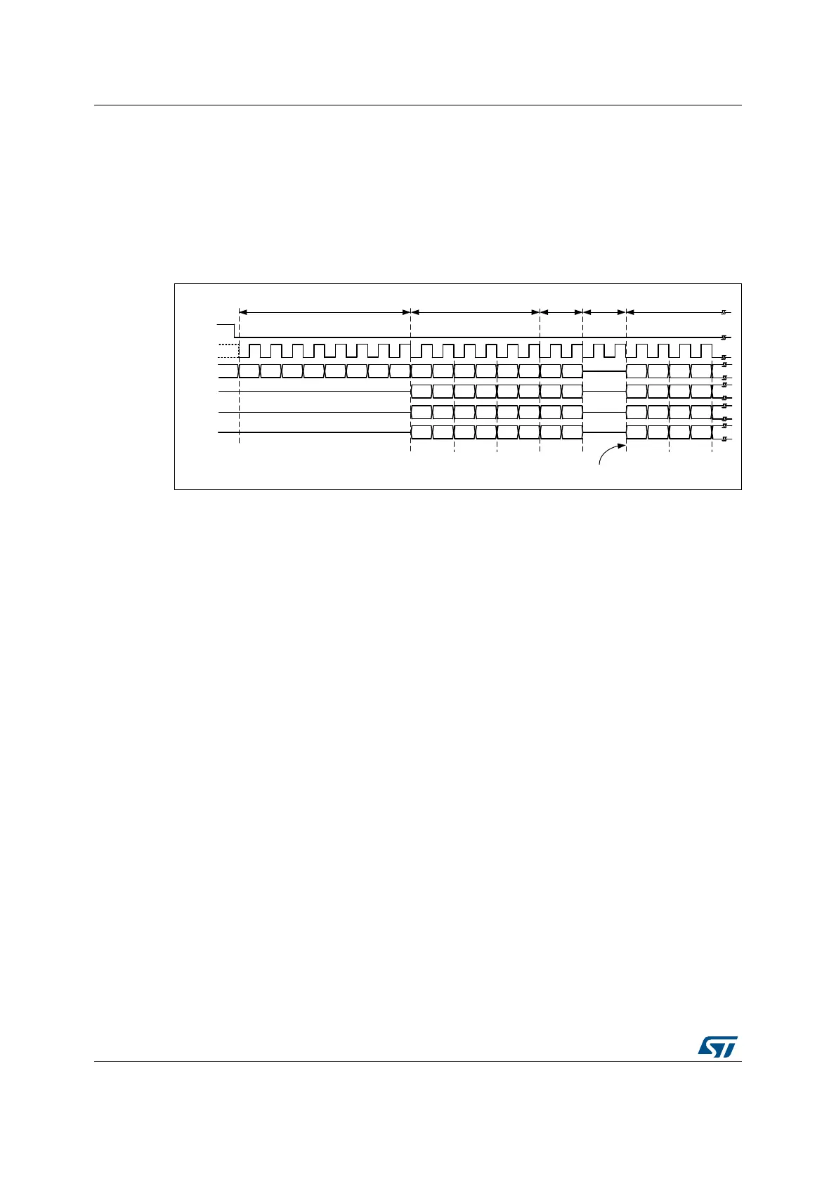
20.3.3 QUADSPI command sequence
The QUADSPI communicates with the Flash memory using commands. Each command
can include 5 phases: instruction, address, alternate byte, dummy, data. Any of these
phases can be configured to be skipped, but at least one of the instruction, address,
alternate byte, or data phase must be present.
nCS falls before the start of each command and rises again after each command finishes.
Figure 76. An example of a read command in quad mode
Instruction phase
During this phase, an 8-bit instruction, configured in INSTRUCTION field of
QUADSPI_CCR[7:0] register, is sent to the Flash memory, specifying the type of operation
to be performed.
Though most Flash memories can receive instructions only one bit at a time from the
IO0/SO signal (single SPI mode), the instruction phase can optionally send 2 bits at a time
(over IO0/IO1 in dual SPI mode) or 4 bits at a time (over IO0/IO1/IO2/IO3 in quad SPI
mode). This can be configured using the IMODE[1:0] field of QUADSPI_CCR[9:8] register.
When IMODE = 00, the instruction phase is skipped, and the command sequence starts
with the address phase, if present.
Address phase
In the address phase, 1-4 bytes are sent to the Flash memory to indicate the address of the
operation. The number of address bytes to be sent is configured in the ADSIZE[1:0] field of
QUADSPI_CCR[13:12] register. In indirect and automatic-polling modes, the address bytes
to be sent are specified in the ADDRESS[31:0] field of QUADSPI_AR register, while in
memory-mapped mode the address is given directly via the AHB (from the Cortex
®
or from
a DMA).
The address phase can send 1 bit at a time (over SO in single SPI mode), 2 bits at a time
(over IO0/IO1 in dual SPI mode), or 4 bits at a time (over IO0/IO1/IO2/IO3 in quad SPI
mode). This can be configured using the ADMODE[1:0] field of QUADSPI_CCR[11:10]
register.
When ADMODE = 00, the address phase is skipped, and the command sequence proceeds
directly to the next phase, if any.
MS35317V1
nCS
SCLK
IO0
IO1
IO2
IO3
4
5
6
7
0
1
2
3
4
5
6
7
0
1
2
3
4
5
6
7
0
1
2
3
4
5
6
7
0
1
2
3
4
5
6
7
0
1
2
3
4
5
6
7
0
1
2
3
A23-16 A15-8 A7-0 M7-0 Byte 1 Byte 2
Instruction Address
Alt. Dummy Data
IO switch from
output to input
76 54 32 10
 Loading...


