RM0440 Rev 4 683/2126
RM0440 Analog-to-digital converters (ADC)
724
Where:
• TS_CAL2 is the temperature sensor calibration value acquired at TS_CAL2_TEMP.
• TS_CAL1 is the temperature sensor calibration value acquired at TS_CAL1_TEMP.
• TS_DATA is the actual temperature sensor output value converted by ADC.
Refer to the device datasheet for more information about TS_CAL1 and TS_CAL2
calibration points.
Note: The sensor has a startup time after waking from power-down mode before it can output V
TS
at the correct level. The ADC also has a startup time after power-on, so to minimize the
delay, the ADEN and VSENSESEL bits should be set at the same time.
The above formula is given for TS_DATA measurement done with the same V
REF+
voltage
as TS_CAL1/TS_CAL2 values. If V
REF+
is different, the formula must be adapted. For
example if V
REF+
= 3.3 V and TS_CAL data are acquired at V
REF+
= 3.0 V, TS_DATA must
be replaced by TS_DATA x (3.3/3.0).
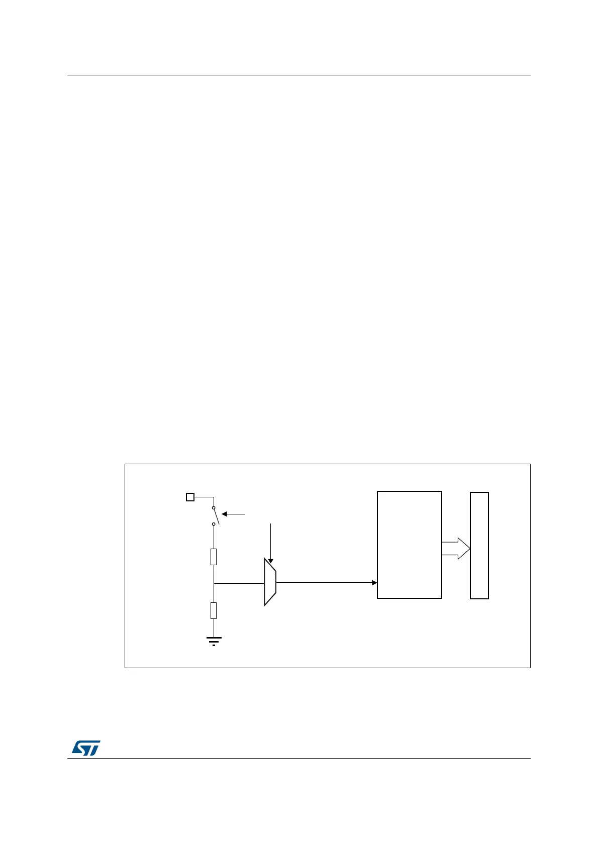
21.4.32 V
BAT
supply monitoring
The VBATSEL bit in the ADCx_CCR register is used to switch to the battery voltage. As the
V
BAT
voltage could be higher than V
DDA
, to ensure the correct operation of the ADC, the
V
BAT
pin is internally connected to a bridge divider by 3. This bridge is automatically enabled
when VBATSEL is set, to connect V
BAT
/3 to the ADC input channels. As a consequence, the
converted digital value is one third of the V
BAT
voltage. To prevent any unwanted
consumption on the battery, it is recommended to enable the bridge divider only when
needed, for ADC conversion.
Refer to the electrical characteristics of the device datasheet for the sampling time value to
be applied when converting the V
BAT
/3 voltage.
The figure below shows the block diagram of the V
BAT
sensing feature.
Figure 154. V
BAT
channel block diagram
1. The VBATSEL bit must be set to enable the conversion of internal channel for V
BAT
/3.
MSv46151V1
V
BAT
V
BAT
/3
VBATSEL
ADCx
ADC input
Address/data bus
 Loading...


