General-purpose timers (TIM2/TIM3/TIM4/TIM5) RM0440
1340/2126 RM0440 Rev 4
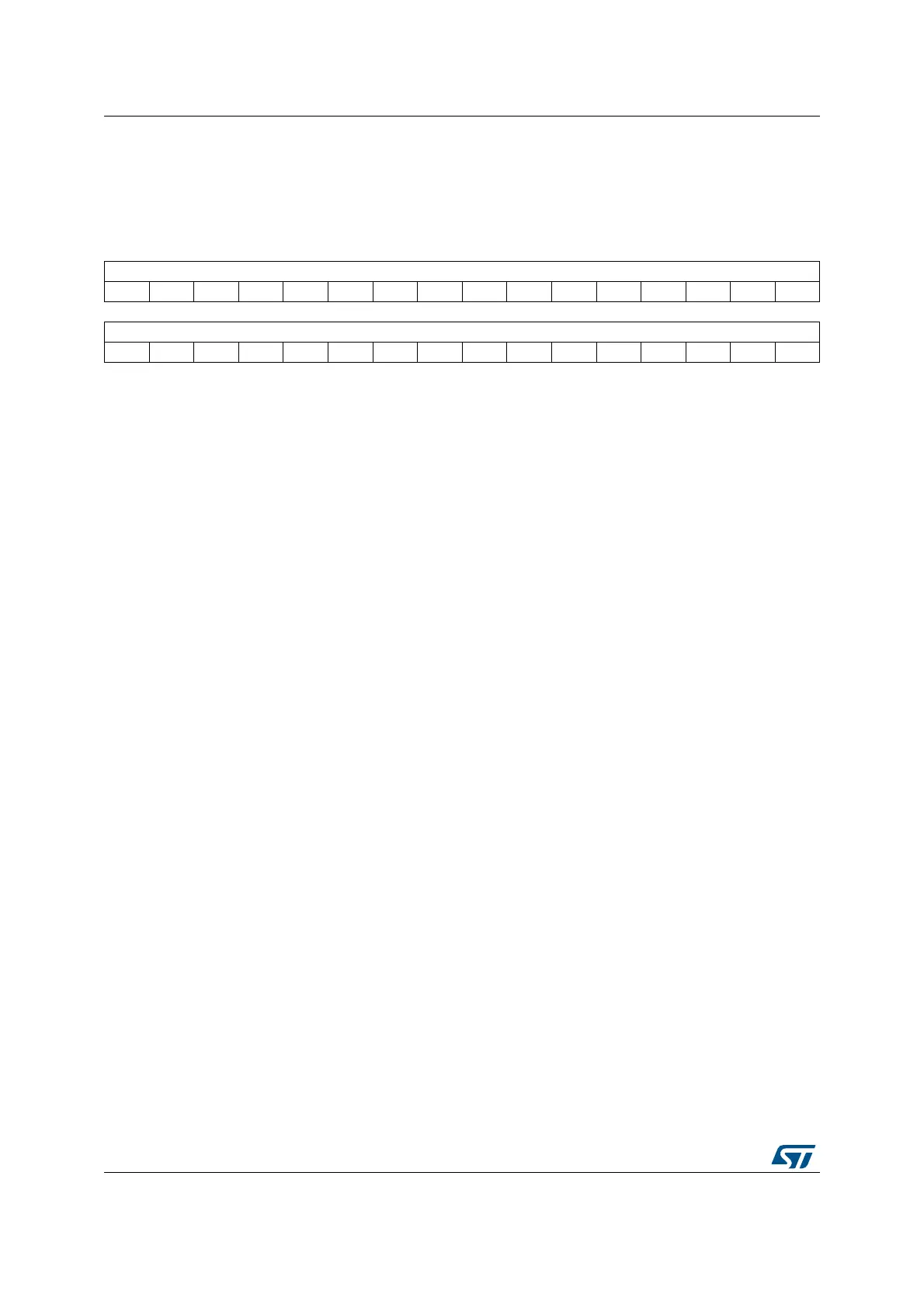
29.5.30 TIMx DMA address for full transfer (TIMx_DMAR)(x = 2 to 5)
Address offset: 0x3E0
Reset value: 0x0000 0000
31 30 29 28 27 26 25 24 23 22 21 20 19 18 17 16
DMAB[31:16]
rw rw rw rw rw rw rw rw rw rw rw rw rw rw rw rw
1514131211109876543210
DMAB[15:0]
rw rw rw rw rw rw rw rw rw rw rw rw rw rw rw rw
Bits 31:0 DMAB[31:0]: DMA register for burst accesses
A read or write operation to the DMAR register accesses the register located at the address
(TIMx_CR1 address) + (DBA + DMA index) x 4
where TIMx_CR1 address is the address of the control register 1, DBA is the DMA base
address configured in TIMx_DCR register, DMA index is automatically controlled by the
DMA transfer, and ranges from 0 to DBL (DBL configured in TIMx_DCR).
 Loading...


