Flexible static memory controller (FSMC) RM0440
564/2126 RM0440 Rev 4
To perform an ECC computation:
1. Enable the ECCEN bit in the FMC_PCR register.
2. Write data to the NAND Flash memory page. While the NAND page is written, the ECC
block computes the ECC value.
3. Read the ECC value available in the FMC_ECCR register and store it in a variable.
4. Clear the ECCEN bit and then enable it in the FMC_PCR register before reading back
the written data from the NAND page. While the NAND page is read, the ECC block
computes the ECC value.
5. Read the new ECC value available in the FMC_ECCR register.
6. If the two ECC values are the same, no correction is required, otherwise there is an
ECC error and the software correction routine returns information on whether the error
can be corrected or not.
19.7.7 NAND Flash controller registers
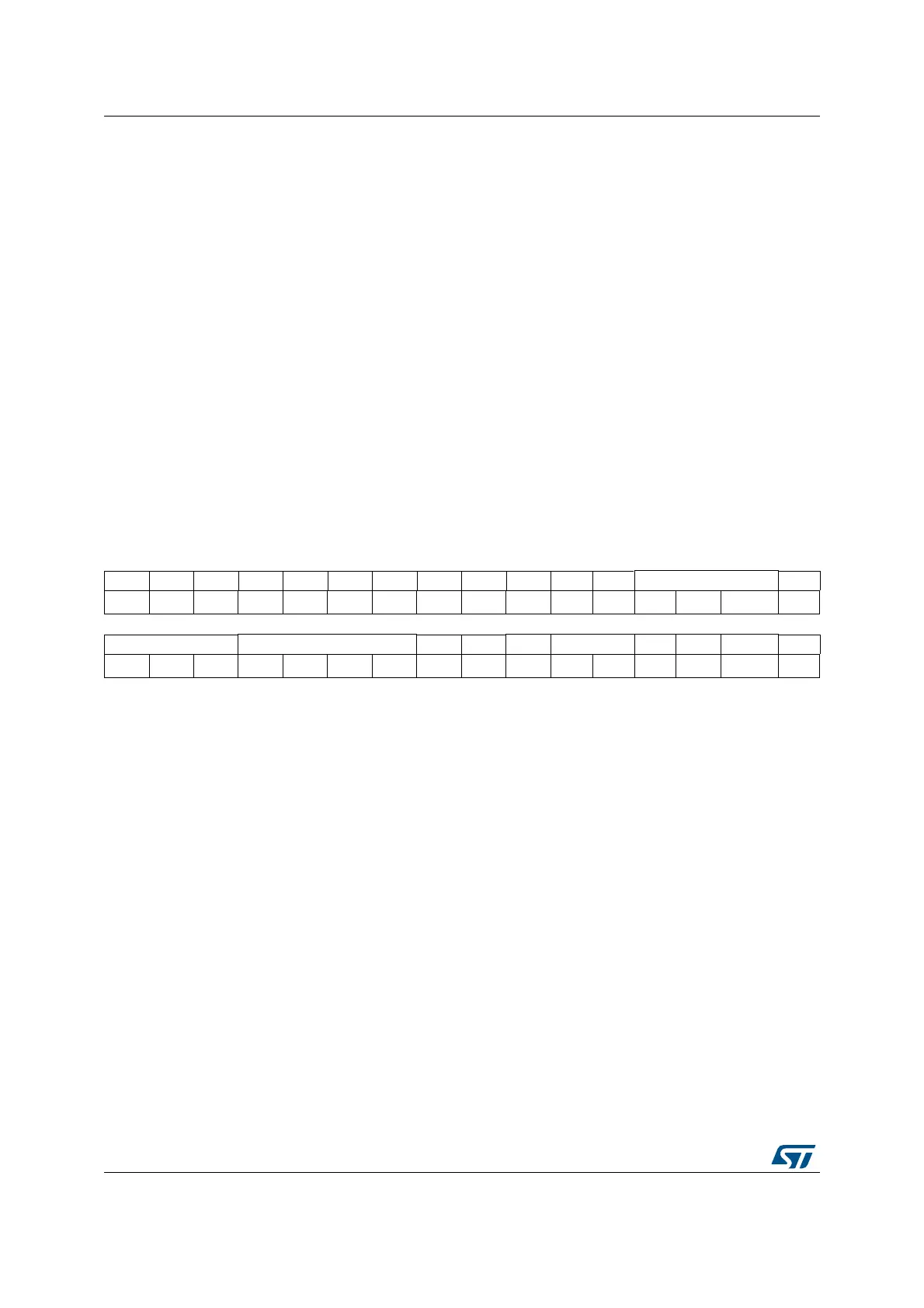
NAND Flash control registers (FMC_PCR)
Address offset: 0x80
Reset value: 0x0000 0018
31 30 29 28 27 26 25 24 23 22 21 20 19 18 17 16
Res. Res. Res. Res. Res. Res. Res. Res. Res. Res. Res. Res. ECCPS[2:0] TAR3
rw rw rw rw
15141312111098765432 1 0
TAR[2:0] TCLR[3:0] Res. Res. ECCEN PWID[1:0] PTYP PBKEN PWAITEN Res.
rw rw rw rw rw rw rw rw rw rw rw rw rw
Bits 31:20 Reserved, must be kept at reset value.
Bits 19:17 ECCPS[2:0]: ECC page size
Defines the page size for the extended ECC:
000: 256 bytes
001: 512 bytes
010: 1024 bytes
011: 2048 bytes
100: 4096 bytes
101: 8192 bytes
Bits 16:13 TAR[3:0]: ALE to RE delay
Sets time from ALE low to RE low in number of AHB clock cycles (HCLK).
Time is: t_ar = (TAR + SET + 2) × THCLK where THCLK is the HCLK clock period
0000: 1 HCLK cycle (default)
1111: 16 HCLK cycles
Note: SET is MEMSET or ATTSET according to the addressed space.
 Loading...


