Analog-to-digital converters (ADC) RM0440
698/2126 RM0440 Rev 4
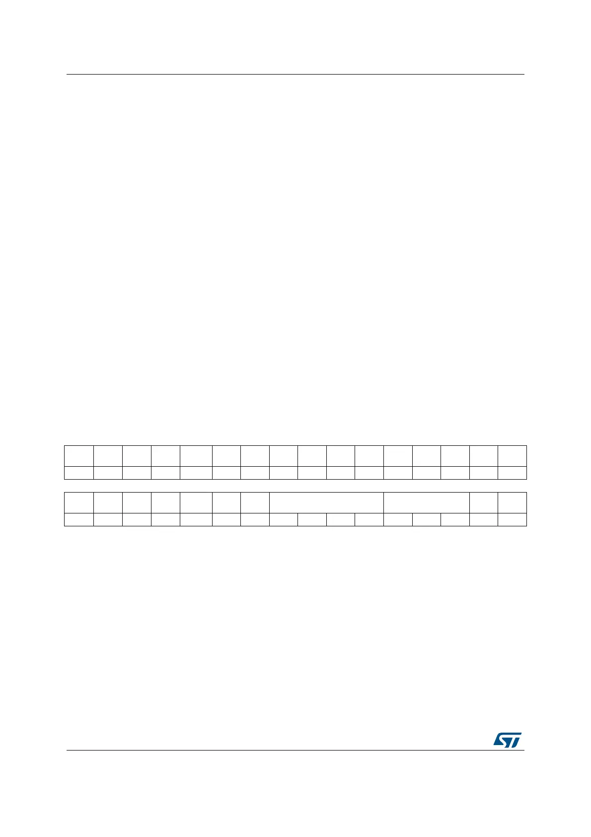
21.6.5 ADC configuration register 2 (ADC_CFGR2)
Address offset: 0x10
Reset value: 0x0000 0000
Bit 2 Reserved, must be kept at reset value.
Bit 1 DMACFG: Direct memory access configuration
This bit is set and cleared by software to select between two DMA modes of operation and is
effective only when DMAEN=1.
0: DMA One Shot mode selected
1: DMA Circular mode selected
For more details, refer to Section : Managing conversions using the DMA
Note: The software is allowed to write this bit only when ADSTART=0 and JADSTART=0 (which
ensures that no conversion is ongoing).
In dual-ADC modes, this bit is not relevant and replaced by control bit DMACFG of the
ADCx_CCR register.
Bit 0 DMAEN: Direct memory access enable
This bit is set and cleared by software to enable the generation of DMA requests. This allows to use
the DMA to manage automatically the converted data. For more details, refer to Section : Managing
conversions using the DMA.
0: DMA disabled
1: DMA enabled
Note: The software is allowed to write this bit only when ADSTART=0 and JADSTART=0 (which
ensures that no conversion is ongoing).
In dual-ADC modes, this bit is not relevant and replaced by control bits MDMA[1:0] of the
ADCx_CCR register.
31 30 29 28 27 26 25 24 23 22 21 20 19 18 17 16
Res. Res. Res. Res.
SMPTRI
G
BULB
SWTRI
G
Res. Res. Res. Res. Res. Res. Res. Res.
GCOM
P
rw rw rw rw
1514131211109876543210
Res. Res. Res. Res. Res.
ROV
SM
TROVS OVSS[3:0] OVSR[2:0] JOVSE ROVSE
rw rw rw rw rw rw rw rw rw rw rw
 Loading...


