Reset and clock control (RCC) RM0351
228/1830 DocID024597 Rev 5
6.4.5 PLLSAI1 configuration register (RCC_PLLSAI1CFGR)
Address offset: 0x10
Reset value: 0x0000 1000
Access: no wait state, word, half-word and byte access
This register is used to configure the PLLSAI1 clock outputs according to the formulas:
• f(VCOSAI1 clock) = f(PLL clock input) × (PLLSAI1N / PLLM)
• f(PLLSAI1_P) = f(VCOSAI1 clock) / PLLSAI1P
• f(PLLSAI1_Q) = f(VCOSAI1 clock) / PLLSAI1Q
• f(PLLSAI1_R) = f(VCOSAI1 clock) / PLLSAI1R
Bits 1:0 PLLSRC: Main PLL, PLLSAI1 and PLLSAI2 entry clock source
Set and cleared by software to select PLL, PLLSAI1 and PLLSAI2 clock source. These bits
can be written only when PLL, PLLSAI1 and PLLSAI2 are disabled.
In order to save power, when no PLL is used, the value of PLLSRC should be 00.
00: No clock sent to PLL, PLLSAI1 and PLLSAI2
01: MSI clock selected as PLL, PLLSAI1 and PLLSAI2 clock entry
10: HSI16 clock selected as PLL, PLLSAI1 and PLLSAI2 clock entry
11: HSE clock selected as PLL, PLLSAI1 and PLLSAI2 clock entry
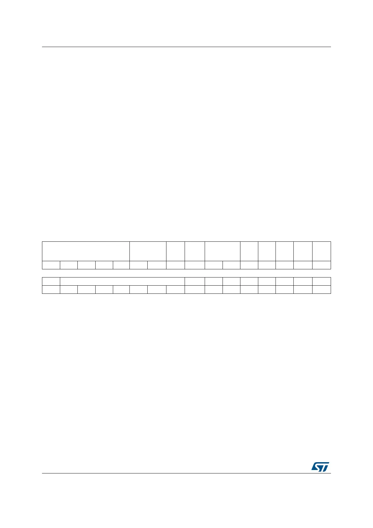
31 30 29 28 27 26 25 24 23 22 21 20 19 18 17 16
PLLSAI1PDIV[4:0] PLLSAI1R[1:0]
PLL
SAI1
REN
Res. PLLSAI1Q[1:0]
PLL
SAI1
QEN
Res. Res.
PLL
SAI1P
PLL
SAI1
PEN
rw rw rw rw rw rw rw rw rw rw rw rw rw
1514131211109 8 7 654321 0
Res. PLLSAI1N[6:0] Res. Res. Res. Res. Res. Res. Res. Res.
rw rw rw rw rw rw rw
 Loading...


