Chrom-Art Accelerator™ controller (DMA2D) RM0351
382/1830 DocID024597 Rev 5
12.5.13 DMA2D background CLUT memory address register
(DMA2D_BGCMAR)
Address offset: 0x0030
Reset value: 0x0000 0000
12.5.14 DMA2D output PFC control register (DMA2D_OPFCCR)
Address offset: 0x0034
Reset value: 0x0000 0000
Bits 31: 0 MA[31: 0]: Memory Address
Address of the data used for the CLUT address dedicated to the foreground image. This
register can only be written when no transfer is ongoing. Once the CLUT transfer has
started, this register is read-only.
If the foreground CLUT format is 32-bit, the address must be 32-bit aligned.
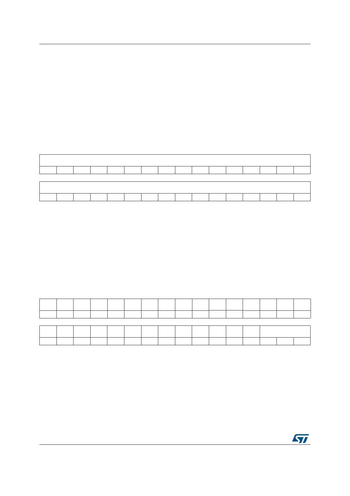
31 30 29 28 27 26 25 24 23 22 21 20 19 18 17 16
MA[31:16]
rw rw rw rw rw rw rw rw rw rw rw rw rw rw rw rw
1514131211109876543210
MA[15:0]
rw rw rw rw rw rw rw rw rw rw rw rw rw rw rw rw
Bits 31: 0 MA[31: 0]: Memory address
Address of the data used for the CLUT address dedicated to the background image.
This register can only be written when no transfer is on going. Once the CLUT transfer
has started, this register is read-only.
If the background CLUT format is 32-bit, the address must be 32-bit aligned.
31 30 29 28 27 26 25 24 23 22 21 20 19 18 17 16
Res. Res. Res. Res. Res. Res. Res. Res. Res. Res. RBS AI Res. Res. Res. Res.
rw rw
1514131211109876543210
Res. Res. Res. Res. Res. Res. Res. Res. Res. Res. Res. Res. Res. CM[2:0]
rw rw rw
 Loading...


