RTC6 boards
Doc. Rev. 1.0.21 en-US
16 Appendix A: The RTC6 Ethernet Board
880
16.2.2 Layout – Lower Side
73
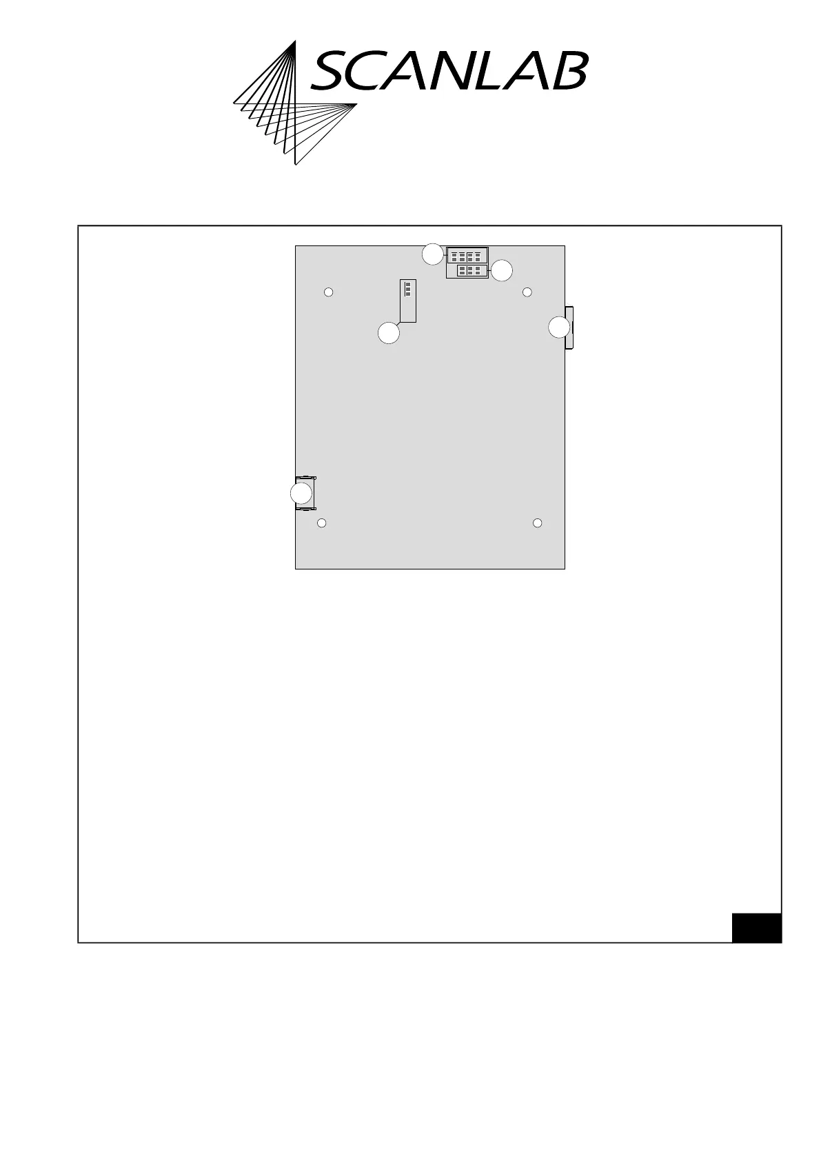
RTC6 Ethernet Board V1.2. Lower side.
16
15
14
13
12
5V3.3V
Digital I/O Voltage
Pin15 Pin17
Latch GND +5V Data7
Slave
1
Legend
12. Solder jumper field A . . . . To configure the level of the output signals at the EXTENSION 1 socket connector.
For details, see “Solder Jumper Field A – Configuring Output Signal Level at EXTENSION 1 Socket
Connector”, page 41.
13. Solder jumper field B . . . . To configure the signal at EXT. 2 socket connector pin (09).
For details, see “Solder Jumper Field B – Configuring pin (09) of EXT. 2 Socket Connector”, page 895.
14. Solder jumper field C . . . . To configure the signal at EXT. 2 socket connector pin (08).
For details, see “Solder Jumper Field C – Configuring Pin (15) of EXTENSION 2 Socket Connector”,
page 43.
15. ETH connector . . . . . . . . . See Figure 72.
16. Slave. . . . . . . . . . . . . . . . . 6-pin socket connector. To connect with another RTC6 board for the purpose of synchronize
clocks. For details, see “Master Socket Connector, Slave Socket Connector”, page 893.