RM0440 Rev 4 109/2126
RM0440 Embedded Flash memory (FLASH) for category 3 devices
228
User and read protection option bytes
Flash memory address: 0x1FFF 7800
ST production value: 0xFFEF F8AA
Bank 2
1FFFF800 Unused
1FFFF808 Unused
Unused and
PCROP2_STRT[14:0]
Unused
Unused and
PCROP2_STRT[14:0]
1FFFF810 Unused
Unused and
PCROP2_END[14:0]
Unused
Unused and
PCROP2_END[14:0]
1FFFF818 Unused
WRP2B
_END
[6:0]
Unused
WRP2B
_STRT
[6:0]
Unused
WRP2B
_END
[6:0]
Unused
WRP2B
_STRT
[6:0]
1FFFF820 Unused
WRP2B
_END
[6:0]
Unused
WRP2B
_STRT
[6:0]
Unused
WRP2B
_END
[6:0]
Unused
WRP2B
_STRT
[6:0]
1FFFF828 Unused
SEC_
_SIZE2
Unused
SEC_
_SIZE2
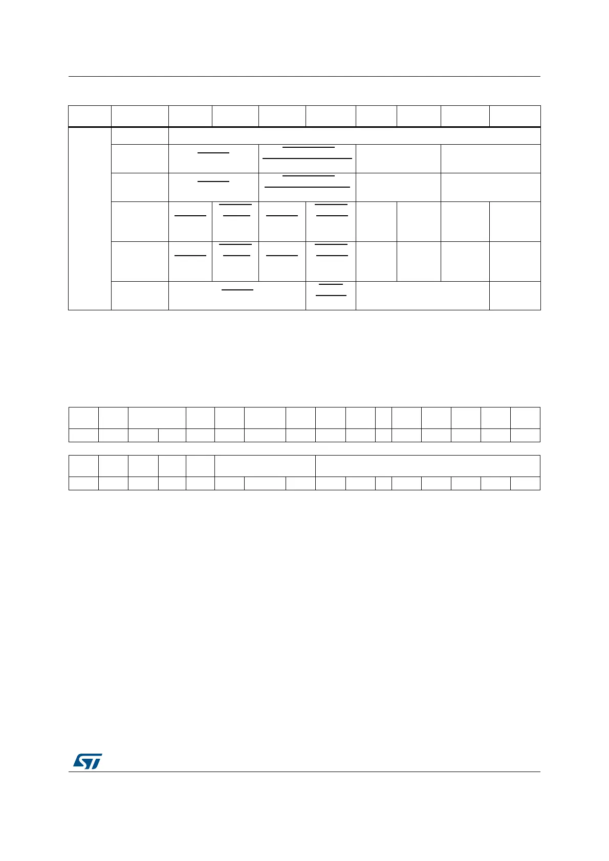
Table 11. Option byte organization (continued)
BANK Address [63:56] [55:48] [47:40] [39:32] [31:24] [23:16] [15:8] [7:0]
31 30 29 28 27 26 25 24 23 22 21 20 19 18 17 16
Res.
IRH_
EN
PG10_
Mode
n
BOOT0
nSW
BOOT0
CCMSRAM
_RST
SRAM
_PE
n
BOOT1
DBANK
Re
s.
BFB2
WWDG
_SW
IWGD_
STDBY
IWDG_
STOP
IWDG_
SW
rrr r r rrr rrrr
15 14 13 12 11 10 9 8 7 6 5 4 3 2 1 0
Res.
nRST_
SHDW
nRST_
STDBY
nRST_
STOP
Res. BOR_LEV[2:0] RDP[7:0]
rrr r r rrrrrrrrr
Bit 31 Reserved, must be kept at reset value.
Bit 30 IRH_IN: Internal reset holder for PG10
0: IRH disabled
1: IRH enabled
Bits 29:28 PG10_Mode: PG10 pad mode
00: Reset Input/Output
01: Reset Input only
10: GPIO
11: Reset Input/Output
Bit 27 nBOOT0: nBOOT0 option bit
0: nBOOT0 = 0
1: nBOOT0 = 1
Bit 26 nSWBOOT0: Software BOOT0
0: BOOT0 taken from the option bit nBOOT0
1: BOOT0 taken from PB8/BOOT0 pin
 Loading...


