RM0440 Rev 4 115/2126
RM0440 Embedded Flash memory (FLASH) for category 3 devices
228
WRP1 Area B address option bytes
Flash memory address: 0x1FFF F818
ST production value: 0xFF00 FFFF
WRP2 Area B address option bytes
Flash memory address: 0x1FFF F820
ST production value: 0xFF00 FFFF
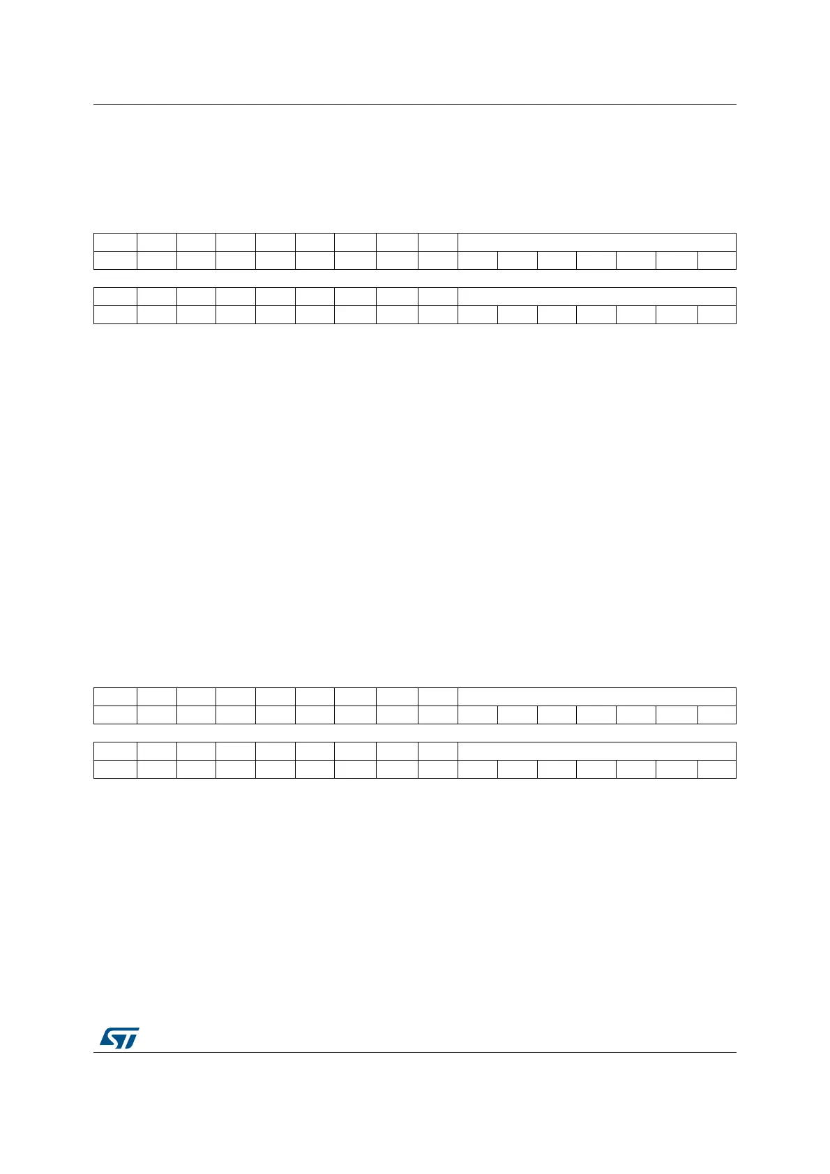
31 30 29 28 27 26 25 24 23 22 21 20 19 18 17 16
Res. Res. Res. Res. Res. Res. Res. Res. Res. WRP1B_END[6:0]
rw rw rw rw rw rw rw
15 14 13 12 11 10 9 8 7 6 5 4 3 2 1 0
Res. Res. Res. Res. Res. Res. Res. Res. Res. WRP1B_STRT[6:0]
rw rw rw rw rw rw rw
Bits 31:23 Reserved, must be kept at reset value.
Bits 22:16 WRP1B_END: WRP first area “B” end offset
DBANK=1
WRP1B_END contains the last page of the WRP first area for bank2.
DBANK=0
WRP1B_END contains the last page of the WRP third area for all memory.
Bits 15:7 Reserved, must be kept at reset value.
Bits 6:0 WRP1B_STRT: WRP first area “B” start offset
DBANK=1
WRP1B_STRT contains the first page of the WRP first area for bank2.
DBANK=0
WRP1B_STRT contains the first page of the WRP third area for all memory.
31 30 29 28 27 26 25 24 23 22 21 20 19 18 17 16
Res. Res. Res. Res. Res. Res. Res. Res. Res. WRP2B_END[6:0]
rw rw rw rw rw rw rw
15 14 13 12 11 10 9 8 7 6 5 4 3 2 1 0
Res. Res. Res. Res. Res. Res. Res. Res. Res. WRP2B_STRT[6:0]
rw rw rw rw rw rw rw
Bits 31:23 Reserved, must be kept at reset value.
 Loading...


