RM0440 Rev 4 1531/2126
RM0440 AES hardware accelerator (AES)
1538
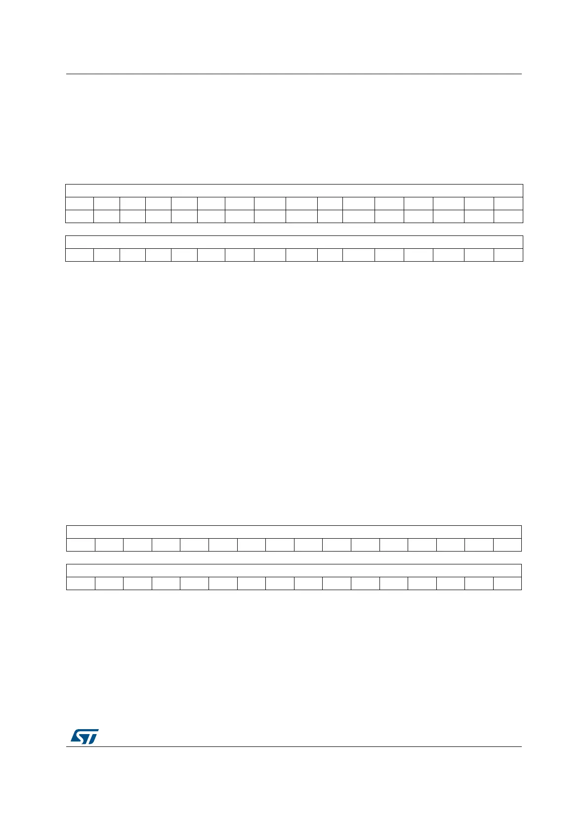
34.7.3 AES data input register (AES_DINR)
Address offset: 0x08
Reset value: 0x0000 0000
Only 32-bit access type is supported.
34.7.4 AES data output register (AES_DOUTR)
Address offset: 0x0C
Reset value: 0x0000 0000
Only 32-bit read access type is supported.
31 30 29 28 27 26 25 24 23 22 21 20 19 18 17 16
DIN[31:16]
rw rw rw rw rw rw rw rw rw rw rw rw rw rw rw rw
15 14 13 12 11 10 9 8 7 6 5 4 3 2 1 0
DIN[15:0]
rw rw rw rw rw rw rw rw rw rw rw rw rw rw rw rw
Bits 31:0 DIN[31:0]: Input data word
A four-fold sequential write to this bitfield during the input phase results in writing a complete 128-bit
block of input data to the AES peripheral. From the first to the fourth write, the corresponding data
weights are [127:96], [95:64], [63:32], and [31:0]. Upon each write, the data from the 32-bit input
buffer are handled by the data swap block according to the DATATYPE[1:0] bitfield, then written into
the AES core 128-bit input buffer.
The data signification of the input data block depends on the AES operating mode:
- Mode 1 (encryption): plaintext
- Mode 2 (key derivation): the bitfield is not used (AES_KEYRx registers used for input)
- Mode 3 (decryption) and Mode 4 (key derivation then single decryption): ciphertext
The data swap operation is described in Section 34.4.13: AES data registers and data swapping on
page 1521.
31 30 29 28 27 26 25 24 23 22 21 20 19 18 17 16
DOUT[31:16]
rrrrrrrrrrrrrrrr
1514131211109876543210
DOUT[15:0]
rrrrrrrrrrrrrrrr
 Loading...


