Inter-integrated circuit (I2C) interface RM0440
1918/2126 RM0440 Rev 4
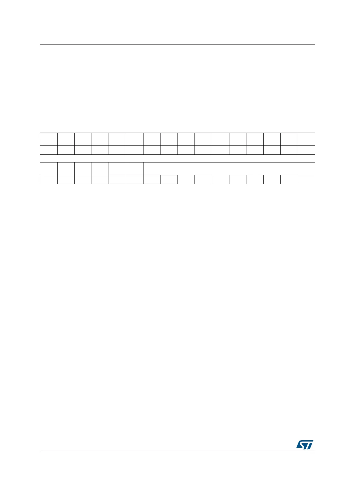
41.7.3 I2C own address 1 register (I2C_OAR1)
Address offset: 0x08
Reset value: 0x0000 0000
Access: No wait states, except if a write access occurs while a write access to this register is
ongoing. In this case, wait states are inserted in the second write access until the previous
one is completed. The latency of the second write access can be up to 2 x PCLK1 + 6 x
I2CCLK.
31 30 29 28 27 26 25 24 23 22 21 20 19 18 17 16
Res. Res. Res. Res. Res. Res. Res. Res. Res. Res. Res. Res. Res. Res. Res. Res.
1514131211109876543210
OA1EN Res. Res. Res. Res.
OA1
MODE
OA1[9:0]
rw rw rw rw rw rw rw rw rw rw rw rw
Bits 31:16 Reserved, must be kept at reset value.
Bit 15 OA1EN: Own Address 1 enable
0: Own address 1 disabled. The received slave address OA1 is NACKed.
1: Own address 1 enabled. The received slave address OA1 is ACKed.
Bits 14:11 Reserved, must be kept at reset value.
Bit 10 OA1MODE: Own Address 1 10-bit mode
0: Own address 1 is a 7-bit address.
1: Own address 1 is a 10-bit address.
Note: This bit can be written only when OA1EN=0.
Bits 9:0 OA1[9:0]: Interface own slave address
7-bit addressing mode: OA1[7:1] contains the 7-bit own slave address. The bits OA1[9],
OA1[8] and OA1[0] are don't care.
10-bit addressing mode: OA1[9:0] contains the 10-bit own slave address.
Note: These bits can be written only when OA1EN=0.
 Loading...


