FD controller area network (FDCAN) RM0440
1986/2126 RM0440 Rev 4
44.4.14 FDCAN transmitter delay compensation register (FDCAN_TDCR)
Address offset: 0x0048
Reset value: 0x0000 0000
44.4.15 FDCAN interrupt register (FDCAN_IR)
The flags are set when one of the listed conditions is detected (edge-sensitive). The flags
remain set until the Host clears them. A flag is cleared by writing a 1 to the corresponding bit
position.
Writing a 0 has no effect. A hard reset clears the register. The configuration of IE controls
whether an interrupt is generated. The configuration of ILS controls on which interrupt line
an interrupt is signaled.
Address offset: 0x0050
Reset value: 0x0000 0000
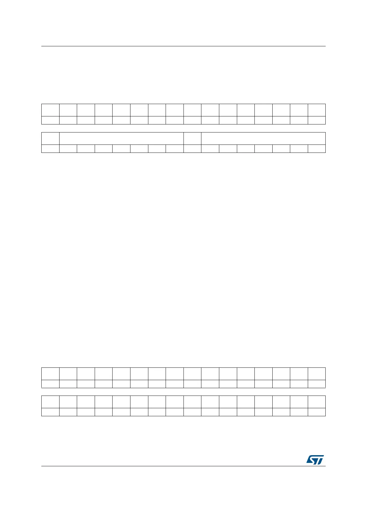
31 30 29 28 27 26 25 24 23 22 21 20 19 18 17 16
Res. Res. Res. Res. Res. Res. Res. Res. Res. Res. Res. Res. Res. Res. Res. Res.
1514131211109876543210
Res. TDCO[6:0] Res. TDCF[6:0]
rw rw rw rw rw rw rw rw rw rw rw rw rw rw
Bits 31:15 Reserved, must be kept at reset value.
Bits 14:8 TDCO[6:0]: Transmitter delay compensation offset
Offset value defining the distance between the measured delay from FDCAN_TX to
FDCAN_RX and the secondary sample point. Valid values are 0 to 127 mtq.
These are protected write (P) bits, which means that write access by the bits is possible only
when the bit 1 [CCE] and bit 0 [INIT] of CCCR register are set to 1.
Bit 7 Reserved, must be kept at reset value.
Bits 6:0 TDCF[6:0]: Transmitter delay compensation filter window length
Defines the minimum value for the SSP position, dominant edges on FDCAN_RX that would
result in an earlier SSP position are ignored for transmitter delay measurements.
These are protected write (P) bits, which means that write access by the bits is possible only
when the bit 1 [CCE] and bit 0 [INIT] of CCCR register are set to 1.
31 30 29 28 27 26 25 24 23 22 21 20 19 18 17 16
Res. Res. Res. Res. Res. Res. Res. Res. ARA PED PEA WDI BO EW EP ELO
rc_w1 rc_w1 rc_w1 rc_w1 rc_w1 rc_w1 rc_w1 rc_w1
1514131211109876543210
TOO MRAF TSW TEFL TEFF TEFN TFE TCF TC HPM RF1L RF1F RF1N RF0L RF0F RF0N
rc_w1 rc_w1 rc_w1 rc_w1 rc_w1 rc_w1 rc_w1 rc_w1 rc_w1 rc_w1 rc_w1 rc_w1 rc_w1 rc_w1 rc_w1 rc_w1
 Loading...


