RM0440 Rev 4 555/2126
RM0440 Flexible static memory controller (FSMC)
571
SRAM/NOR-Flash write timing registers x (FMC_BWTRx)
Address offset: 0x104 + 8 * (x – 1), (x = 1 to 4)
Reset value: 0x0FFF FFFF
This register contains the control information of each memory bank. It is used for SRAMs,
PSRAMs and NOR Flash memories. When the EXTMOD bit is set in the FMC_BCRx
register, then this register is active for write access.
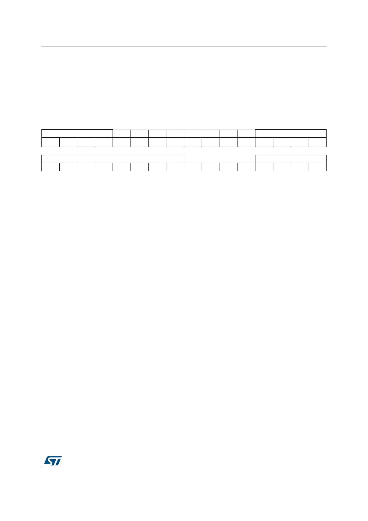
31 30 29 28 27 26 25 24 23 22 21 20 19 18 17 16
DATAHLD[1:0] ACCMOD[1:0] Res. Res. Res. Res. Res. Res. Res. Res. BUSTURN[3:0]
rw rw rw rw rw rw rw rw
1514131211109876543210
DATAST[7:0] ADDHLD[3:0] ADDSET[3:0]
rw rw rw rw rw rw rw rw rw rw rw rw rw rw rw rw
Bits 31:30 DATAHLD[1:0]: Data hold phase duration
These bits are written by software to define the duration of the data hold phase in HCLK cycles
(refer to Figure 54 to Figure 66), used in asynchronous write accesses:
00: DATAHLD phase duration = 1 × HCLK clock cycle (default)
01: DATAHLD phase duration = 2 × HCLK clock cycle
10: DATAHLD phase duration = 3 × HCLK clock cycle
11: DATAHLD phase duration = 4 × HCLK clock cycle
Bits 29:28 ACCMOD[1:0]: Access mode.
Specifies the asynchronous access modes as shown in the next timing diagrams.These bits are
taken into account only when the EXTMOD bit in the FMC_BCRx register is 1.
00: Access mode A
01: Access mode B
10: Access mode C
11: Access mode D
Bits 27:20 Reserved, must be kept at reset value.
Bits 19:16 BUSTURN[3:0]: Bus turnaround phase duration
These bits are written by software to add a delay at the end of current write transaction to next
transaction on the same bank.
For FRAM memories, the bus turnaround delay should be configured to match the minimum t
PC
(precharge time) timings. The bus turnaround delay is inserted between any consecutive
transactions on the same bank (read/read, write/write, read/write and write/read). The chip select is
toggling between any consecutive accesses.
(BUSTURN + 1)HCLK period ≥ tPC min
0000: BUSTURN phase duration = 1 HCLK clock cycle added
...
1111: BUSTURN phase duration = 16 x HCLK clock cycles added (default value after reset)
 Loading...


