RM0440 Rev 4 701/2126
RM0440 Analog-to-digital converters (ADC)
724
21.6.6 ADC sample time register 1 (ADC_SMPR1)
Address offset: 0x14
Reset value: 0x0000 0000
21.6.7 ADC sample time register 2 (ADC_SMPR2)
Address offset: 0x18
Reset value: 0x0000 0000
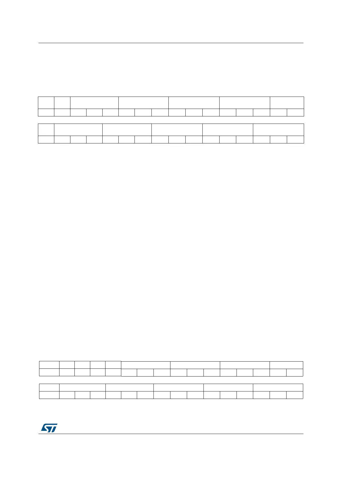
31 30 29 28 27 26 25 24 23 22 21 20 19 18 17 16
SMPPL
US
Res. SMP9[2:0] SMP8[2:0] SMP7[2:0] SMP6[2:0] SMP5[2:1]
rw rw rw rw rw rw rw rw rw rw rw rw rw rw rw
1514131211109876543210
SMP5[
0]
SMP4[2:0] SMP3[2:0] SMP2[2:0] SMP1[2:0] SMP0[2:0]
rw rw rw rw rw rw rw rw rw rw rw rw rw rw rw rw
Bits 31:30 SMPPLUS: Addition of one clock cycle to the sampling time
1: 2.5 ADC clock cycle sampling time becomes 3.5 ADC clock cycles for the ADC_SMPR1
and ADC_SMPR2 registers.
0: The sampling time remains set to 2.5 ADC clock cycles remains
To make sure no conversion is ongoing, the software is allowed to write this bit only when
ADSTART= 0 and JADSTART= 0.
Bit 30 Reserved, must be kept at reset value.
Bits 29:0 SMP[9:0][2:0]: Channel x sampling time selection
These bits are written by software to select the sampling time individually for each channel.
During sample cycles, the channel selection bits must remain unchanged.
000: 2.5 ADC clock cycles
001: 6.5 ADC clock cycles
010: 12.5 ADC clock cycles
011: 24.5 ADC clock cycles
100: 47.5 ADC clock cycles
101: 92.5 ADC clock cycles
110: 247.5 ADC clock cycles
111: 640.5 ADC clock cycles
Note: The software is allowed to write these bits only when ADSTART=0 and JADSTART=0
(which ensures that no conversion is ongoing).
Some channels are not connected physically. Keep the corresponding SMPx[2:0]
setting to the reset value.
31 30 29 28 27 26 25 24 23 22 21 20 19 18 17 16
Res. Res. Res. Res. Res. SMP18[2:0] SMP17[2:0] SMP16[2:0] SMP15[2:1]
rw rw rw rw rw rw rw rw rw rw rw
15 14 13 12 11 10 9 8 7 6 5 4 3 2 1 0
SMP15[0] SMP14[2:0] SMP13[2:0] SMP12[2:0] SMP11[2:0] SMP10[2:0]
rw rw rw rw rw rw rw rw rw rw rw rw rw rw rw rw
 Loading...


