5-56 Bus Interface
AMD-K5 Processor Technical Reference Manual 18524C/0—Nov1996
During burst reads the processor drives BE7–BE0 to identify
only the byte address of the next desired operand. The byte
indication does not change throughout the burst; it continues
to be driven on BE7–BE0 during all four transfers. The memory
subsystem must ignore BE7–BE0 during the second, third, and
fourth transfers of a burst and return all eight bytes corre-
sponding to the eight-byte address on A31–A3. Furthermore,
the memory subsystem must determine the successive
addresses, depending on the starting address that the proces-
sor drives on A31–A3, as described in Table 5-4 on page 5-21.
During writebacks the processor drives all bits of BE7–BE0
Low to indicate that all eight bytes on D63–D0 are valid. Write-
backs are addressed by A31–A3, but they are always aligned to
32-byte boundaries so that A4–A3 are always 0.
If memory reads, memory writes, or I/O reads are misaligned,
the Pentium processor transfers the highest-addressed portion
followed by the lowest-addressed portion. The AMD-K5 proces-
sor runs such cycles in the opposite order from the Pentium
processor. I/O writes, however, are performed in the same
order on both processors.
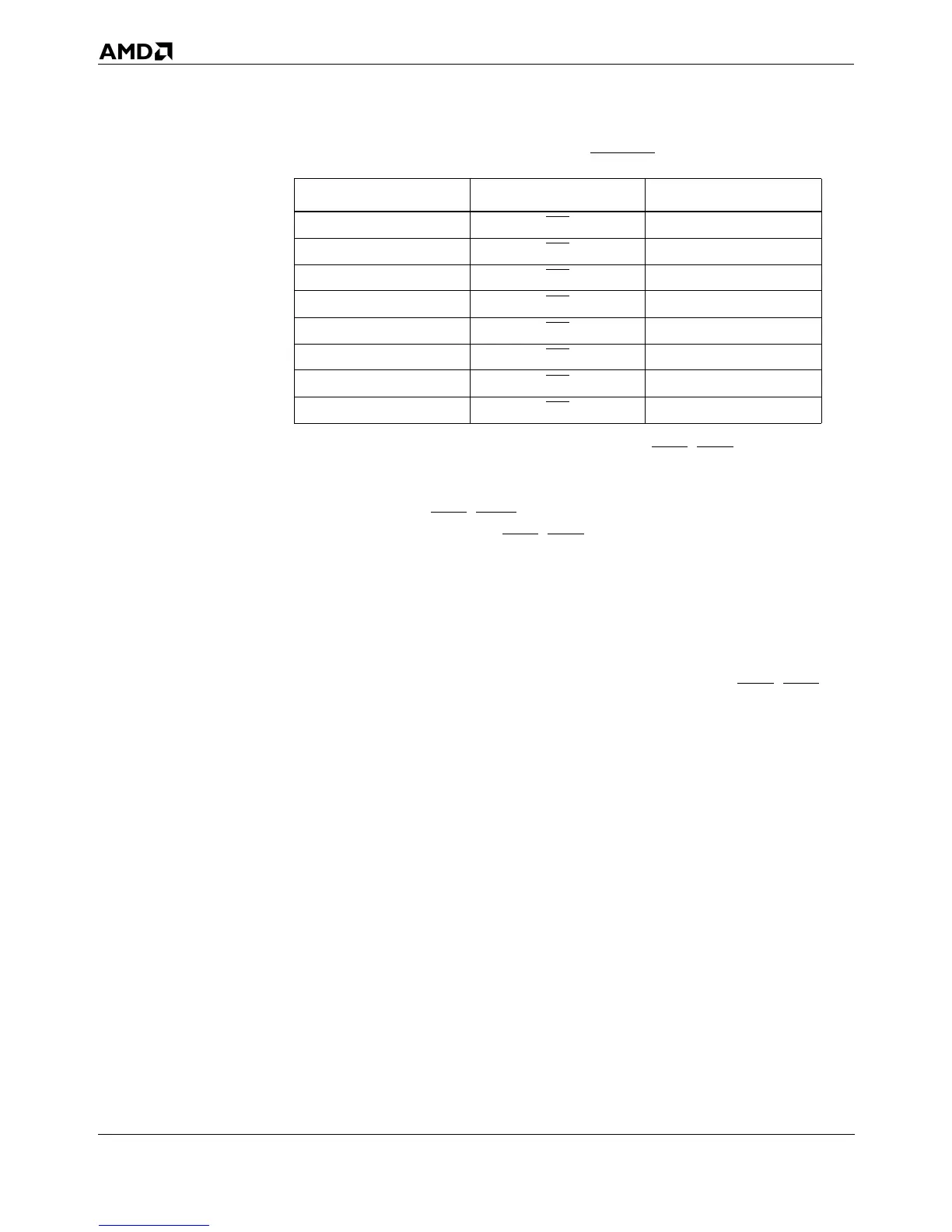
Table 5-10. Relation Between D63–D0, BE7–BE0, and DP7–DP0
Byte On Data Bus Byte Enable Output Data Parity Bits
D63–D56 BE7
DP7
D55–D48 BE6
DP6
D47–D40 BE5
DP5
D39–D32 BE4
DP4
D31–D24 BE3
DP3
D23–D16 BE2
DP2
D15–D8 BE1
DP1
D7–D0 BE0
DP0