Bus Cycle Timing 5-185
18524C/0—Nov1996 AMD-K5 Processor Technical Reference Manual
Cache-Writeback
and Invalidation
Cycle (WBINVD
Instruction)
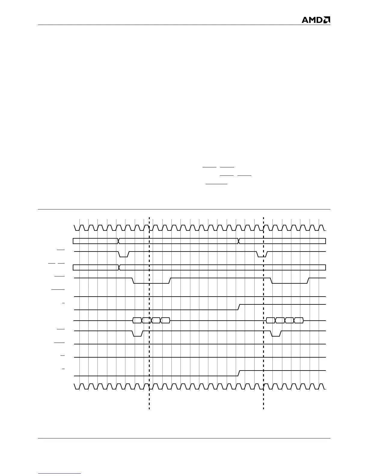
Figure 5-24A and Figure 5-24B show the cache-writeback and
invalidation special bus cycle, followed by the cache-invalida-
tion special bus cycle. The processor drives these two special
cycles after executing the WBINVD instruction.
The execution of WBINVD causes the processor to invalidate
each line in its instruction and data caches. If a data cache line
is in the modified state, the line is written back immediately
before being invalidated. During such writebacks, A31–A5
defines the address of a 32-byte location in memory to which
the modified cache line will be written back. After all modified
lines are written back and all lines in both caches are invali-
dated, the processor first drives the cache-writeback and inval-
idation special bus cycle (BE7–BE0 = F7h) and then the cache-
invalidation special bus cycle (BE7–BE0 = FDh). System logic
must respond by asserting BRDY to each of the two special
cycles as shown in Figure 5-24B.
Figure 5-24A. Cache-Writeback and Invalidation Cycle (WBINVD Instruction) Part 1
CLK
A31–A3
ADS
BE7–BE0
BRDY
CACHE
D/C
D63–D0
KEN
LOCK
M/IO
W/R
CLK
WBINVD
Instruction
Completes
Writeback