5-136 Bus Interface
AMD-K5 Processor Technical Reference Manual 18524C/0—Nov1996
5.3 Bus Cycle Overview
The bus signals described in the previous section combine to
form various types of bus transactions, or bus cycles. This sec-
tion summarizes the general features of the bus cycles: cycle
definition, addressing, alignment, and priorities. Section 5.4
describes the signal timing for specific types of bus cycles.
5.3.1 Cycle Definitions
The processor begins driving a bus cycle when it asserts ADS.
Concurrent with ADS, it drives the set of signals indicated in
Table 5-19, which define the type of bus cycle. For memory
reads, memory writes, burst reads, and burst writes, D/C speci-
fies whether the bus cycle accesses code (instructions) or data.
M/IO specifies whether the cycle accesses memory or an I/O
port. W/R specifies whether the cycle is a read or write. The
assertion of CACHE indicates that the processor is writing or is
prepared to read a burst cycle consisting of four consecutive
transfers on the data bus. However, for a read, system logic
must confirm the burst by asserting KEN, or the bus cycle
becomes a single-transfer read. I/O accesses are always non-
burst cycles.
Interrupt acknowledge operations consist of a locked pair of
read cycles. Special bus cycles are further differentiated by
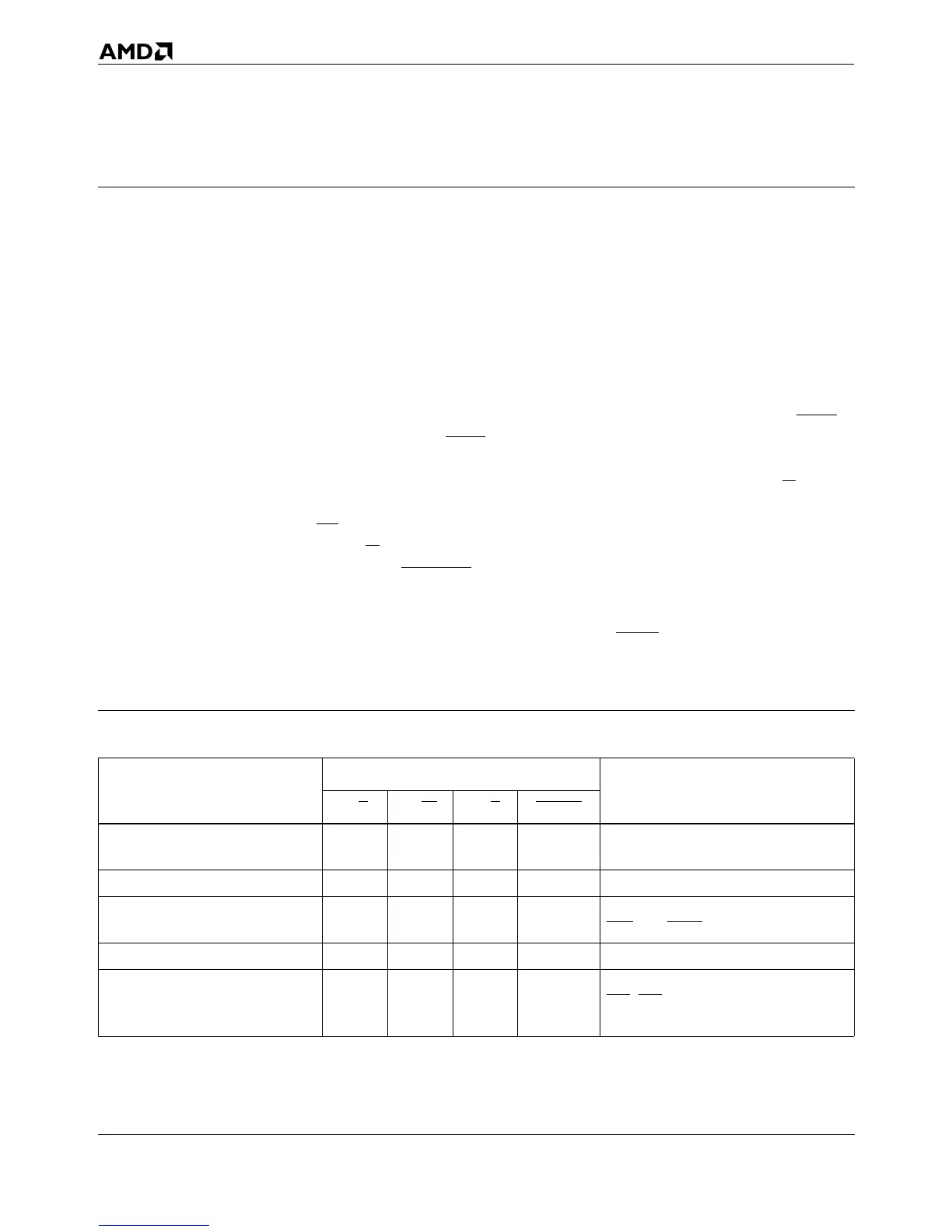
Table 5-19. Bus Cycle Definitions
Type of Cycle
Signals
Comments
D/C
M/IO W/R CACHE
Single-Transfer Memory Read or
Write
0 or 1 1 0 or 1 1 —
Single-Transfer I/O Read or Write 1 0 0 or 1 1 —
Burst Memory Read or Write 0 or 1 1 0 or 1 0
For reads, system logic must assert
KEN
with BRDY.
Interrupt Acknowledge 0 0 0 — Pair of locked cycles.
Special 0 0 1 —
Several special cycles distinguished by
BE7
–BE0 and A31–A3. See Table 5-23
on page 5-180.