Model-Specific Registers (MSRs) 3-27
18524C/0—Nov1996 AMD-K5 Processor Technical Reference Manual
3.2.3 Time Stamp Counter (TSC)
With each processor clock cycle, the processor increments a 64-
bit time stamp counter (TSC) model-specific register. The
counter can be written or read using the WRMSR or RDMSR
instructions when the ECX register contains the value 10h and
CPL = 0. The counter can also be read using the RDTSC
instruction (see Section 3.3.4 on page 3-32) but the required
privilege level for this instruction is determined by the Time
Stamp Disable (TSD) bit in CR4. With any of these instruc-
tions, the EDX and EAX registers hold the upper and lower
double-words (dwords) of the 64-bit value to be written to or
read from the TSC, as follows:
■ EDX—Upper 32 bits of TSC
■ EAX—Lower 32 bits of TSC
The TSC can be loaded with any arbitrary value.
3.2.4 Array Access Register (AAR)
The Array Access Register (AAR) contains pointers for testing
the tag and data arrays for the instruction cache, data cache, 4-
Kbyte TLB, and 4-Mbyte TLB. The AAR can be written or read
with the WRMSR or RDMSR instruction when the ECX regis-
ter contains the value 82h.
For details on the AAR, see Section 7.4 on page 7-7.
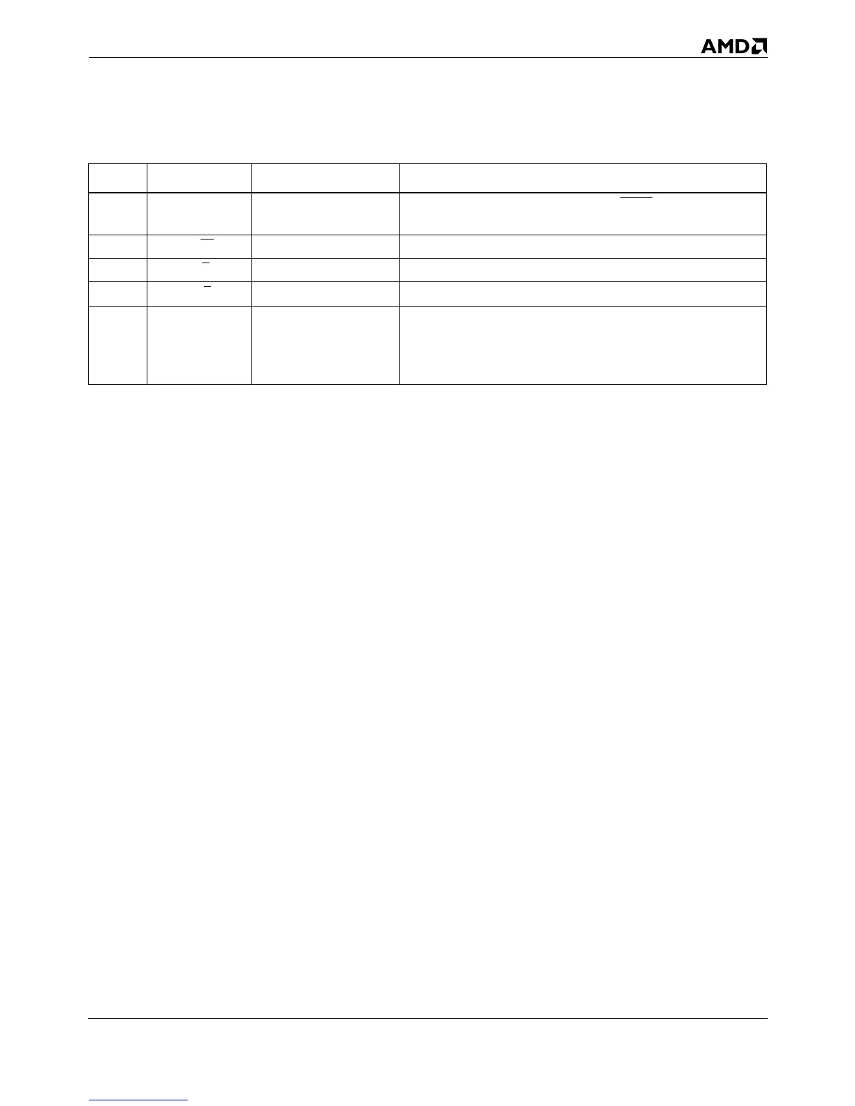
Table 3-7. Machine-Check Type Register (MCTR) Fields
Bit Mnemonic Description Function
4 LOCK Locked Cycle
Set to 1 if the processor was asserting LOCK
during the bus
cycle.
3M/IO
Memory or I/O 1 = memory cycle, 0 = I/O cycle.
2D/C
Data or Code 1 = data cycle, 0 = code cycle.
1W/R
Write or Read 1 = write cycle, 0 = read cycle.
0CHK
Valid Machine-Check
Data
The processor sets the CHK bit to 1 when both the MCTR and
MCAR registers contain valid information. The processor clears
the CHK bit to 0 when software reads the MCTR with the
RDMSR instruction.