EasyManuals Logo

AMD K5 User Manual

AMD K5
406 pages
To Next Page IconTo Next Page
To Previous Page IconTo Previous Page
Page #297 background imageLoading...
Page #297 background image
Bus Cycle Timing 5-181
18524C/0Nov1996 AMD-K5 Processor Technical Reference Manual
Basic Special Bus
Cycle
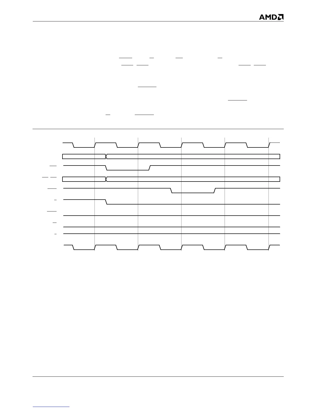
Figure 5-20 shows a basic special bus cycle, which is defined
during ADS by D/C = 0, M/IO = 0, and W/R = 1 and differenti-
ated by BE7–BE0 and A31–A3. In this example, BE7–BE0
= FBh and A31–A3 = 0, so it is the special cycle the processor
generates after executing a HLT instruction. System logic must
respond with BRDY.
All special bus cycles serialize the pipeline. EWBE is not
checked prior to running special bus cycles (all of which have
W/R =1), so EWBE has no effect on any special bus cycles.
Figure 5-20. Basic Special Bus Cycle (Halt Cycle)
CLK
A31–A3
ADS
BE7–BE0
BRDY
D/C
EWBE
M/IO
W/R
CLK

Table of Contents

Questions and Answers:

Question and Answer IconNeed help?

Do you have a question about the AMD K5 and is the answer not in the manual?

AMD K5 Specifications

General IconGeneral
ManufacturerAMD
ModelK5
Architecturex86
MicroarchitectureK5
Introduction Year1996
Clock Speed75 - 133 MHz
Core Count1
SocketSocket 7
Core steppingSSA/5, 5k86
Voltage3.3V
Transistors4.3 million
L1 Cache8 KB (data) + 16 KB (instruction)
FSB50 MHz to 66 MHz
Process Technology350 nm

Related product manuals