5-150 Bus Interface
AMD-K5 Processor Technical Reference Manual 18524C/0—Nov1996
In the clock after ADS, the processor drives the first of four
sequential eight-byte (quadword) transfers on the data bus.
The processor holds the first transfer on the bus until system
logic returns BRDY, then it transfers the next quadword. In
this example, system logic returns BRDY with no wait states,
and the processor responds by driving the subsequent quad-
word in the next clock. Typical systems, however, add one or
more wait states between the transfers.
For both read cycles, the processor asserts CACHE with ADS
and system logic asserts KEN with the BRDY of the first trans-
fer. Thus, CACHE and KEN agree, and the access is cached.
This agreement between CACHE and KEN is required in order
for a burst read to occur. The processor only drives burst reads
if the access is cacheable. If either CACHE or KEN were
negated during the BRDY of the first transfer, the read would
terminate with the first quadword transfer, thus becoming a
single-transfer read.
In this example, the processor negates PWT (indicating write-
back state) and system logic drives WB/WT High with the
BRDY of the first transfer (also indicating writeback state).
Thus, PWT and WB/WT agree, and the cache line becomes a
writeback line, which is cached in the exclusive MESI state.
Details on the writeback/writethrough and MESI cache-coher-
ency state transitions are given in Table 2-2 on page 2-19.
In Figure 5-7, the two consecutive burst reads are identical to
those in Figure 5-6, except that system logic asserts NA one
clock before it asserts BRDY in the first read cycle of Figure
5-7. This causes KEN and WB/WT to be effective when NA
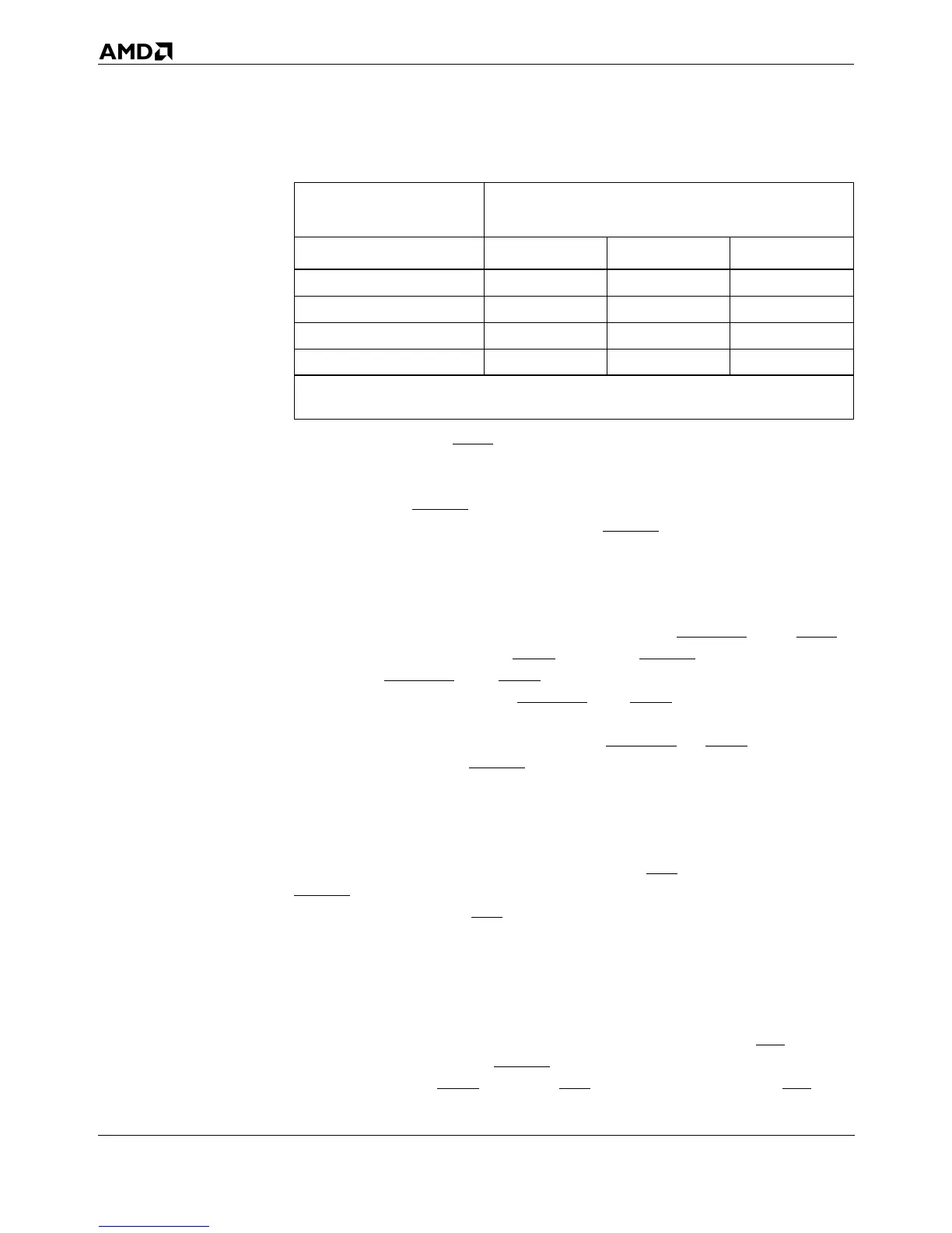
Table 5-21. Address-Generation Sequence During Bursts
Address Driven By
Processor on A31–A3
Addresses of Subsequent Quadwords
1
Generated By System Logic
Quadword 1 Quadword 2 Quadword 3 Quadword 4
...00h ...08h ...10h ...18h
...08h ...00h ...18h ...10h
...10h ...18h ...00h ...08h
...18h ...10h ...08h ...00h
Notes:
1. quadword = 8 bytes