5-146 Bus Interface
AMD-K5 Processor Technical Reference Manual 18524C/0—Nov1996
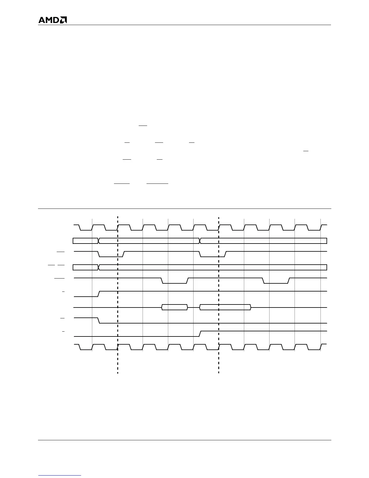
I/O Read and Write Figure 5-4 shows an I/O read followed by an I/O write. The pro-
cessor accesses I/O when it executes an I/O instruction (any of
the INx or OUTx instructions). Accesses to memory-mapped
I/O ports appear on the bus as accesses to memory rather than
to the I/O address space.
The I/O-cycle protocol is nearly the same as the protocol for
read and write accesses to memory, shown in Figure 5-2, except
that M/IO = 0. Only data (not code) can be read or written from
the I/O address space. The cycle definition for an I/O code read
(D/C = 0, M/IO = 0, W/R = 0) defines an interrupt acknowledge
cycle, and the cycle-definition for an I/O code write (D/C =0,
M/IO = 0, W/R = 1) defines a special bus cycle.
The example in Figure 5-4 shows a single wait state separating
ADS and BRDY for the read. In actual systems, however, the
time will typically be longer.
Figure 5-4. I/O Read and Write
CLK
A31–A3
ADS
BE7–BE0
BRDY
D/C
D63–D0
M/IO
W/R
CLK
Read Write