5-4 Bus Interface
AMD-K5 Processor Technical Reference Manual 18524C/0—Nov1996
5.1.1 Signal Characteristics
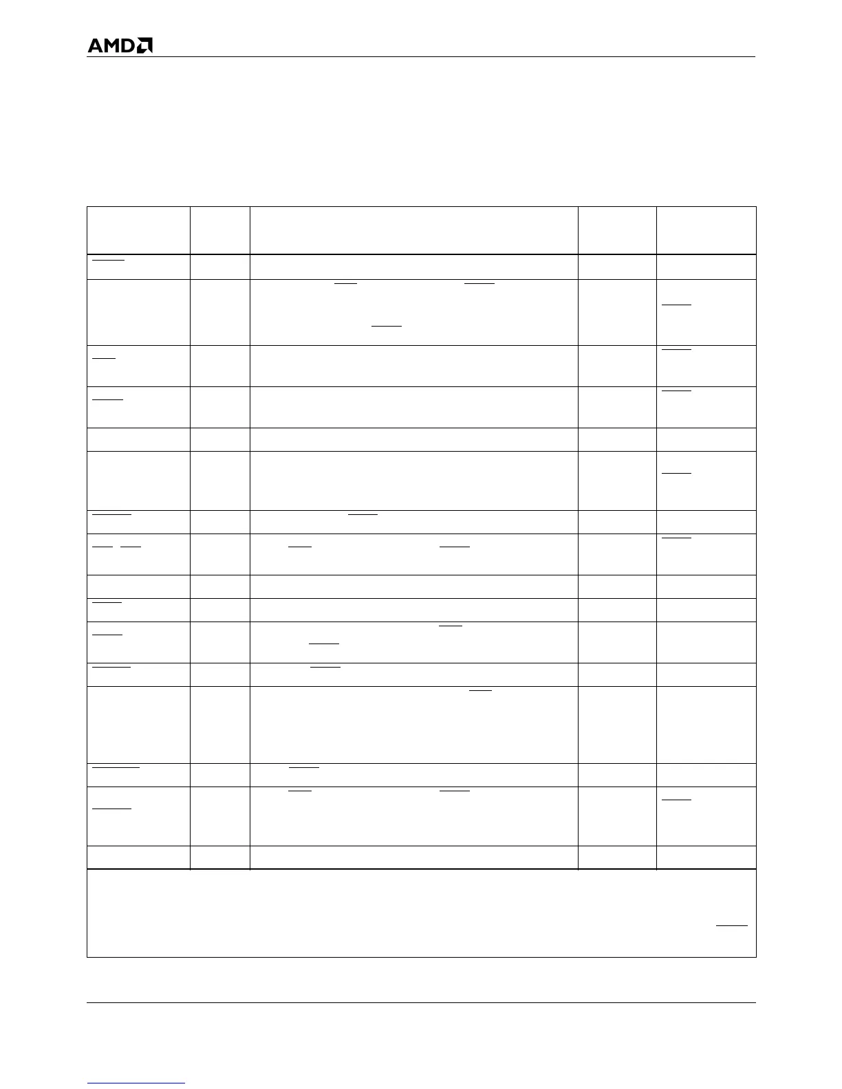
Table 5-1. Summary of Signal Characteristics
Signal Type
Sampled (Input) or
Asserted (Output)
2
Internal
Resistor
Floated
3
A20M
1
IEvery clock.
A31–A3 I/O
Output: From ADS
until last expected BRDY of the bus
cycle.
Input: Same clock as EADS
. A4–A3 are disabled for input.
AHOLD +1,
BOFF
+1 or
HLDA
ADS
O First clock of bus cycle.
BOFF
+1 or
HLDA
ADSC
O First clock of bus cycle.
BOFF
+1 or
HLDA
AHOLD I Every clock.
AP I/O (same as A31–A3)
AHOLD +1,
BOFF
+1 or
HLDA
APCHK
O Two clocks after EADS, for one clock.
BE7
–BE0 OFrom ADS until the last expected BRDY of the bus cycle.
BOFF
+1 or
HLDA
BF (BF1–BF0) I Falling edge of RESET. pullup
BOFF
I Every clock.
BRDY
I
Every clock, from one clock after ADS
until the last
expected BRDY
of the bus cycle.
BRDYC
I (same as BRDY) pullup
BREQ O
First clock of every bus cycle (same as ADS
), cache store,
cache-tag recovery, and aliased cache load. Asserted con-
tinuously while processor is held off bus and needs
access to continue.
BUSCHK
I Every BRDY. Recognized at the next instruction boundary. pullup
CACHE
O
From ADS
until the last expected BRDY of the bus cycle.
Driven for all reads; only driven for writes during write-
backs.
BOFF
+1 or
HLDA
CLK I Always.
Notes:
1. Can be driven asynchronously or synchronously.
2. The term clock means bus clock (CLK). “+n” means n CLKs later.
3. “+n” means n CLKs after the named signal is sampled active. All outputs and bidirectionals are floated during the float test (FLUSH
at RESET).