Signal Overview 5-5
18524C/0—Nov1996 AMD-K5 Processor Technical Reference Manual
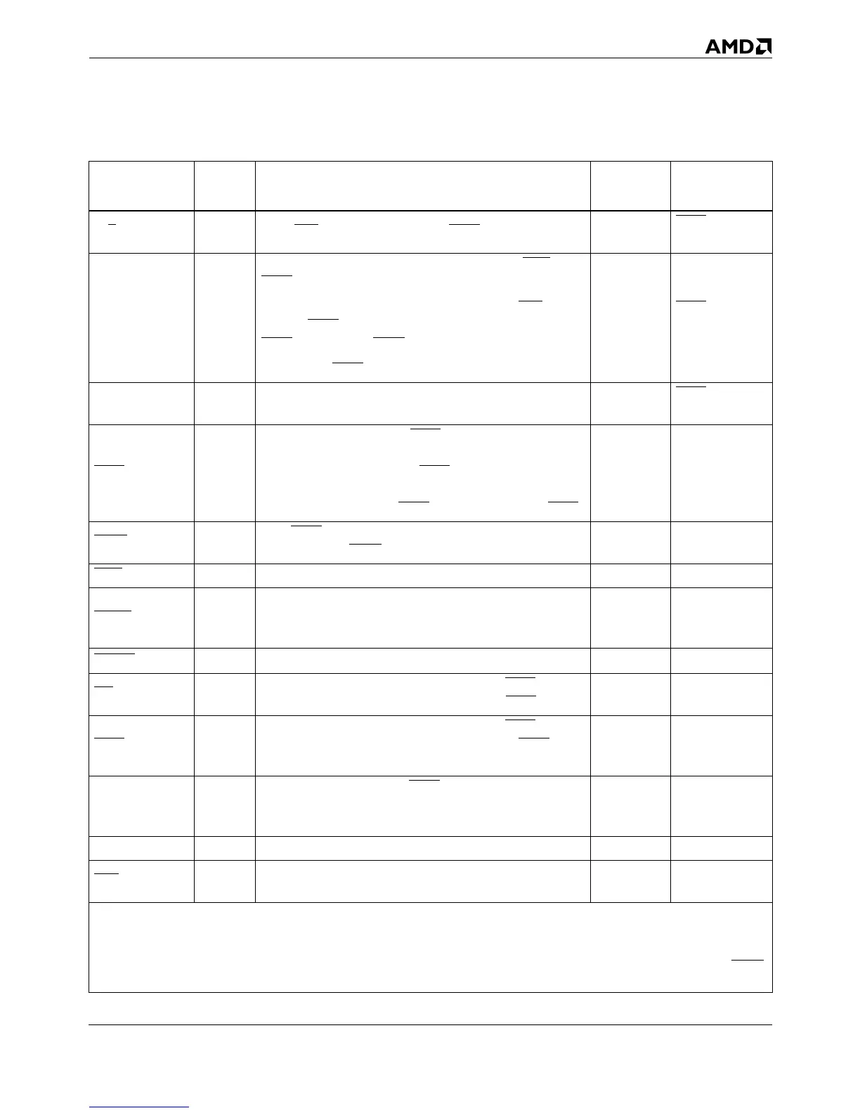
D/C OFrom ADS until the last expected BRDY of the bus cycle.
BOFF
+1 or
HLDA
D63–D0 I/O
Output (single transfer): From one clock after ADS
until
BRDY
.
Output (burst transfer): From one clock after ADS
until
the first BRDY
, and thereafter from one clock after each
BRDY
until the next BRDY.
Input: Every BRDY
.
BOFF
+1 or
HLDA
DP7–DP0 I/O (same as D63–D0)
BOFF
+1 or
HLDA
EADS
I
Every clock while AHOLD, BOFF
or HLDA is asserted,
beginning two clocks after the assertion of AHOLD, two
clocks after the assertion of BOFF
, or one clock after the
assertion of HLDA; except while the processor drives
A31–A3, while it asserts HITM
, and one clock after EADS.
EWBE
I
With BRDY
of external write cycles and in every clock
thereafter until EWBE
is asserted.
FERR
O Every clock.
FLUSH
1
I
Every clock. Falling-edge-triggered. Recognized at next
instruction boundary. Acknowledged with Flush-Acknowl-
edge special bus cycle.
FRCMC
1
I Every clock in which RESET is asserted.
HIT
O
Every clock. Changes state two clocks after EADS
and
retains that state until two clocks after next EADS
.
HITM
O
Every clock. Changes state two clocks after EADS
and
retains that state until one clock after the last BRDY
of
writeback.
HLDA O
From two clocks after last BRDY
of an in-progress bus
cycle, or two clocks after HOLD, whichever comes last,
until two clocks after HOLD is negated.
HOLD I Every clock. Acknowledged with HLDA.
IERR
O
Every clock, in the Functional-Redundancy Checking
mode.
Table 5-1. Summary of Signal Characteristics (continued)
Signal Type
Sampled (Input) or
Asserted (Output)
2
Internal
Resistor
Floated
3
Notes:
1. Can be driven asynchronously or synchronously.
2. The term clock means bus clock (CLK). “+n” means n CLKs later.
3. “+n” means n CLKs after the named signal is sampled active. All outputs and bidirectionals are floated during the float test (FLUSH
at RESET).