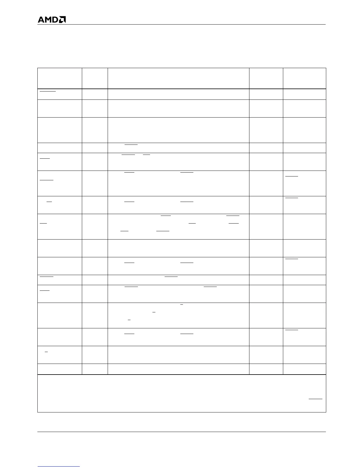
5-6 Bus Interface
AMD-K5 Processor Technical Reference Manual 18524C/0—Nov1996
IGNNE
1
I Every clock.
INIT
1
I
Every clock. Rising-edge-triggered. Recognized at next
instruction boundary.
INTR
1
I
Every clock. Level-sensitive. Recognized at next instruc-
tion boundary. Acknowledged with an interrupt acknowl-
edge operation.
INV I Every EADS
.
KEN
I
First BRDY
or NA of bus cycle, whichever comes first. Rec-
ognized only during read cycles.
LOCK
O
From ADS
until last expected BRDY of the bus cycle.
Negated for one clock (dead cycle) between sequential
locked operations.
BOFF
+1 or
HLDA
M/IO
OFrom ADS until last expected BRDY of the bus cycle.
BOFF
+1 or
HLDA
NA
I
From one clock after ADS
until the first expected BRDY of
a bus cycle. The only function of NA
is to validate KEN or
WB/WT
in place of BRDY.
NMI
1
I
Every clock. Rising-edge-triggered. Recognized at next
instruction boundary.
PCD O From ADS
until last expected BRDY of the bus cycle.
BOFF
+1 or
HLDA
PCHK
O Two clocks after every BRDY of read cycles.
PEN
I
Every BRDY
of read cycles, and second BRDY of interrupt
acknowledge operation.
PRDY O
Every clock, in response to R/S
. Asserted at instruction
boundary after R/S
is sampled Low. Negated in the clock
after R/S
is sampled High.
PWT O From ADS
until last expected BRDY of the bus cycle.
BOFF
+1 or
HLDA
R/S
1
I
Every clock. Level-sensitive. Recognized at next instruc-
tion boundary. Acknowledged with PRDY.
pullup
RESET
1
I Every clock. Recognized at next instruction boundary.
Table 5-1. Summary of Signal Characteristics (continued)
Signal Type
Sampled (Input) or
Asserted (Output)
2
Internal
Resistor
Floated
3
Notes:
1. Can be driven asynchronously or synchronously.
2. The term clock means bus clock (CLK). “+n” means n CLKs later.
3. “+n” means n CLKs after the named signal is sampled active. All outputs and bidirectionals are floated during the float test (FLUSH
at RESET).