EasyManuals Logo

AMD K5 User Manual

AMD K5
406 pages
To Next Page IconTo Next Page
To Previous Page IconTo Previous Page
Page #319 background imageLoading...
Page #319 background image
Memory 6-7
18524C/0Nov1996 AMD-K5 Processor Technical Reference Manual
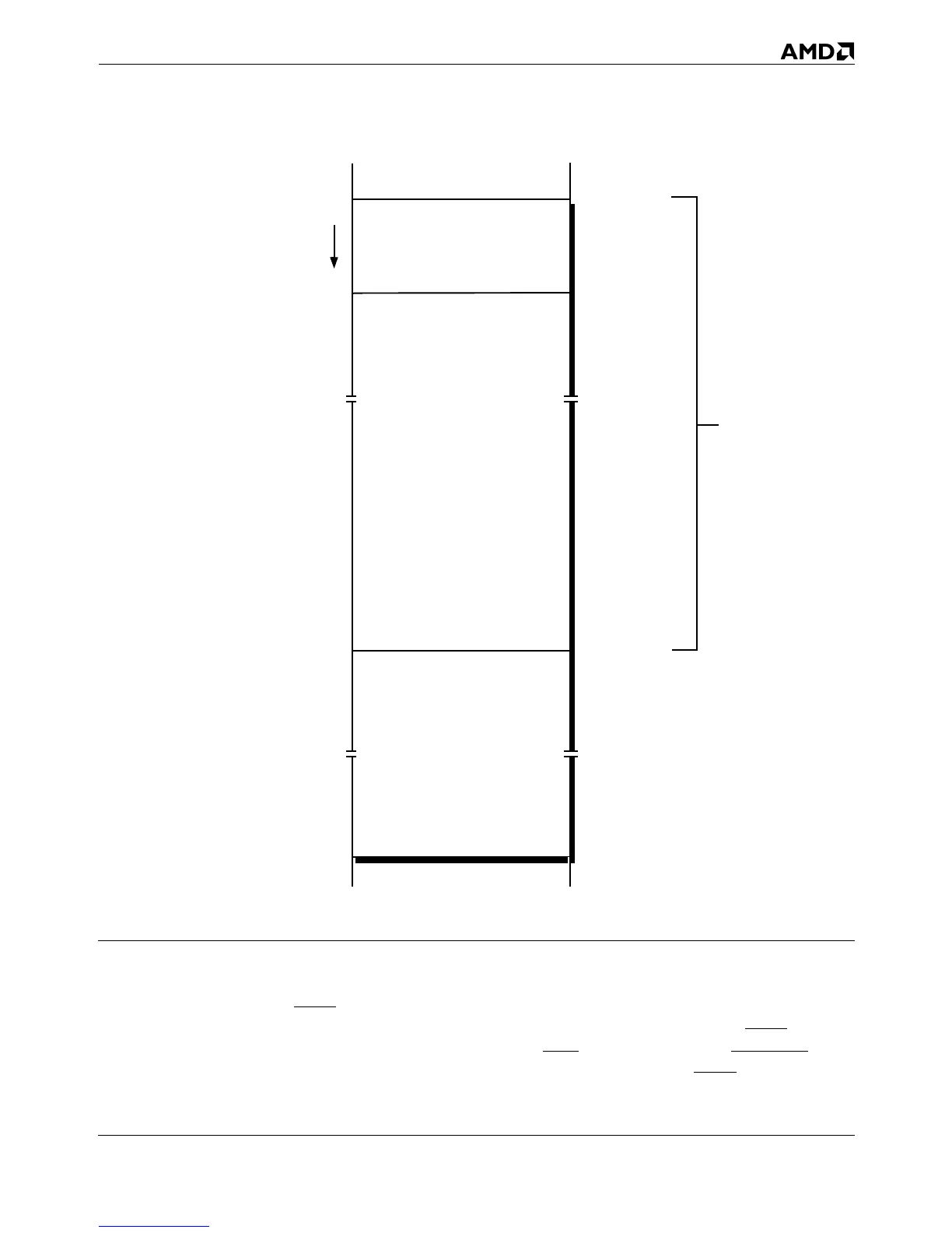
Figure 6-2. Default SMM Memory Map
System logic controls the cacheability of SMM memory with
KEN in the same way that it controls the cacheability of mem-
ory space. If SMM memory is to be non-cacheable, KEN must
be held negated from when SMI is asserted until SMIACT is
negated. If SMM memory is to be cacheable, KEN must be
asserted for cacheable read cycles.
SMM
State-Save
Area
SMM Base Address (CS)
Service Routine Entry Point
Fill Down
SMM
Service Routine
32-Kbyte
Minimum
RAM
0003_8000
0003_FE00
0003_FFFF
0003_0000

Table of Contents

Questions and Answers:

Question and Answer IconNeed help?

Do you have a question about the AMD K5 and is the answer not in the manual?

AMD K5 Specifications

General IconGeneral
ManufacturerAMD
ModelK5
Architecturex86
MicroarchitectureK5
Introduction Year1996
Clock Speed75 - 133 MHz
Core Count1
SocketSocket 7
Core steppingSSA/5, 5k86
Voltage3.3V
Transistors4.3 million
L1 Cache8 KB (data) + 16 KB (instruction)
FSB50 MHz to 66 MHz
Process Technology350 nm

Related product manuals