Control Register 4 (CR4) Extensions 3-11
18524C/0—Nov1996 AMD-K5 Processor Technical Reference Manual
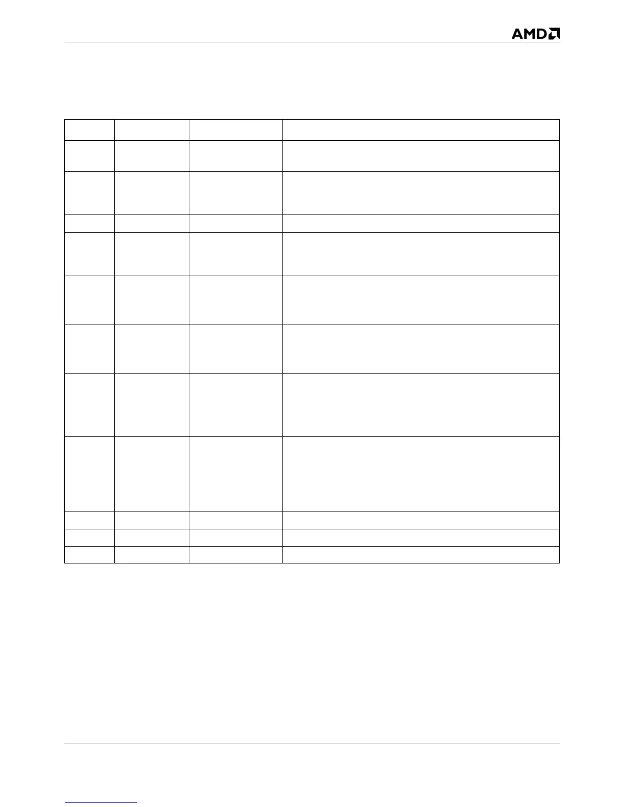
Table 3-3. Page-Table Entry (PTE) Fields
Bit Mnemonic Description Function
31–12 BASE
Physical Base
Address
The physical base address of a 4-Kbyte page.
11–9 AVL
Available to Soft-
ware
Software may use the field to store any type of information.
When the page-table entry is not present (P bit cleared), bits 31–1
become available to software.
8 G Global 0 = local, 1 = global.
7 PS Page Size
This bit is ignored in page-table entries, although clearing it to 0
preserves consistent usage of this bit between page-table and
page-directory entries.
6 D Dirty
The processor sets this bit to 1 during a write to the page that is
mapped by this page-table entry.
0 = not written, 1 = written.
5AAccessed
The processor sets this bit to 1 during a read or write to any page
that is mapped by this page-table entry.
0 = not read or written, 1 = read or written.
4 PCD Page Cache Disable
Specifies cacheability for all locations in the page mapped by this
page-table entry. Whether a location is actually cached also
depends on several other factors.
0 = cacheable page, 1 = non-cacheable.
3 PWT Page Writethrough
Specifies writeback or writethrough cache protocol for all loca-
tions in the page mapped by this page-table entry. Whether a
location is actually cached in a writeback or writethrough state
also depends on several other factors.
0 = writeback, 1 = writethough.
2 U/S User/Supervisor 0 = user (any CPL), 1 = supervisor (CPL < 3).
1 W/R Write/Read 0 = read or execute, 1 = write, read, or execute.
0 P Present 0 = not valid, 1 = valid.