RM0440 Rev 4 1417/2126
RM0440 General-purpose timers (TIM15/TIM16/TIM17)
1445
30.7.21 TIM15 DMA control register (TIM15_DCR)
Address offset: 0x3DC
Reset value: 0x0000 0000
30.7.22 TIM15 DMA address for full transfer (TIM15_DMAR)
Address offset: 0x3E0
Reset value: 0x0000 0000
Bits 15:0 Reserved, must be kept at reset value.
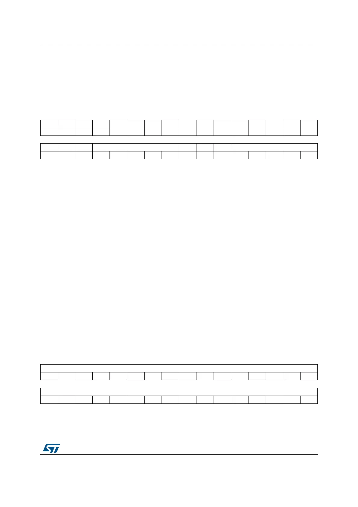
31 30 29 28 27 26 25 24 23 22 21 20 19 18 17 16
Res. Res. Res. Res. Res. Res. Res. Res. Res. Res. Res. Res. Res. Res. Res. Res.
1514131211109876543210
Res. Res. Res. DBL[4:0] Res. Res. Res. DBA[4:0]
rw rw rw rw rw rw rw rw rw rw
Bits 31:13 Reserved, must be kept at reset value.
Bits 12:8 DBL[4:0]: DMA burst length
This 5-bit field defines the length of DMA transfers (the timer recognizes a burst transfer
when a read or a write access is done to the TIM15_DMAR address).
00000: 1 transfer,
00001: 2 transfers,
00010: 3 transfers,
...
10001: 18 transfers.
Bits 7:5 Reserved, must be kept at reset value.
Bits 4:0 DBA[4:0]: DMA base address
This 5-bit field defines the base-address for DMA transfers (when read/write access are
done through the TIM15_DMAR address). DBA is defined as an offset starting from the
address of the TIM15_CR1 register.
Example:
00000: TIM15_CR1,
00001: TIM15_CR2,
00010: TIM15_SMCR,
...
31 30 29 28 27 26 25 24 23 22 21 20 19 18 17 16
DMAB[31:16]
rw rw rw rw rw rw rw rw rw rw rw rw rw rw rw rw
1514131211109876543210
DMAB[15:0]
rw rw rw rw rw rw rw rw rw rw rw rw rw rw rw rw
 Loading...


