Embedded Flash memory (FLASH) for category 2 devices RM0440
202/2126 RM0440 Rev 4
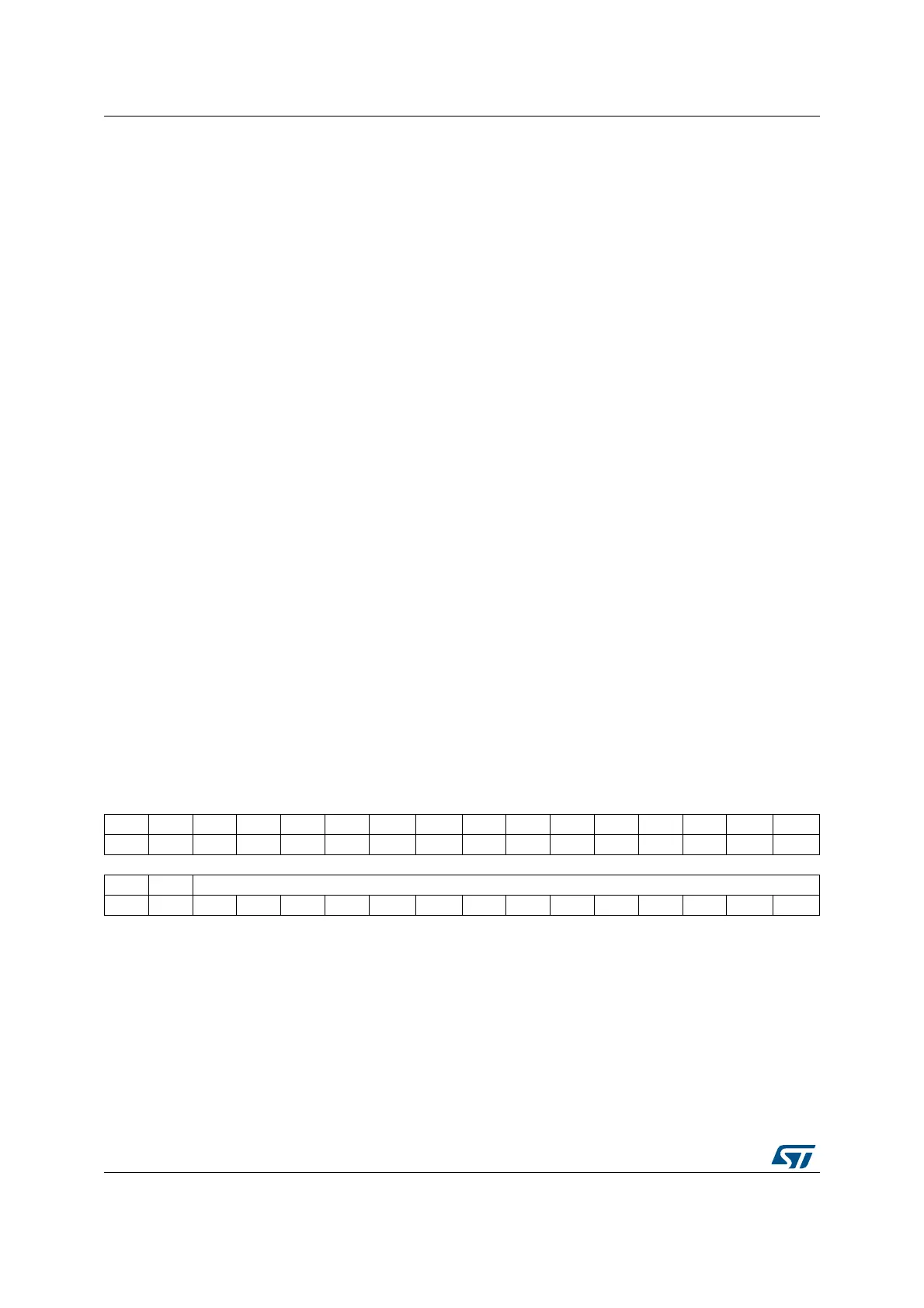
PCROP1 Start address option bytes
Flash memory address: 0x1FFF 7808
ST production value: 0xFFFF FFFF
PCROP1 End address option bytes
Flash memory address: 0x1FFF 7810
ST production value: 0x00FF 0000
Bit 16 IDWG_SW: Independent watchdog selection
0: Hardware independent watchdog
1: Software independent watchdog
Bit 15 Reserved, must be kept at reset value.
Bit 14 nRST_SHDW
0: Reset generated when entering the Shutdown mode
1: No reset generated when entering the Shutdown mode
Bit 13 nRST_STDBY
0: Reset generated when entering the Standby mode
1: No reset generate when entering the Standby mode
Bit 12 nRST_STOP
0: Reset generated when entering the Stop mode
1: No reset generated when entering the Stop mode
Bit 11 Reserved, must be kept at reset value.
Bits10:8 BOR_LEV: BOR reset Level
These bits contain the VDD supply level threshold that activates/releases the
reset.
000: BOR Level 0. Reset level threshold is around 1.7 V
001: BOR Level 1. Reset level threshold is around 2.0 V
010: BOR Level 2. Reset level threshold is around 2.2 V
011: BOR Level 3. Reset level threshold is around 2.5 V
100: BOR Level 4. Reset level threshold is around 2.8 V
Bits 7:0 RDP: Read protection level
0xAA: Level 0, read protection not active
0xCC: Level 2, chip read protection active
Others: Level 1, memories read protection active
31 30 29 28 27 26 25 24 23 22 21 20 19 18 17 16
Res. Res. Res. Res. Res. Res. Res. Res. Res. Res. Res. Res. Res. Res. Res. Res.
1514131211109 8 765432 1 0
Res. Res. PCROP1_STRT[13:0]
rw rw rw rw rw rw rw rw rw rw rw rw rw rw
Bits 31:14 Reserved, must be kept at reset value.
Bits 13:0 PCROP1_STRT: PCROP area start offset
PCROP1_STRT contains the first double-word of the PCROP area for bank1.
 Loading...


