RM0440 Rev 4 203/2126
RM0440 Embedded Flash memory (FLASH) for category 2 devices
228
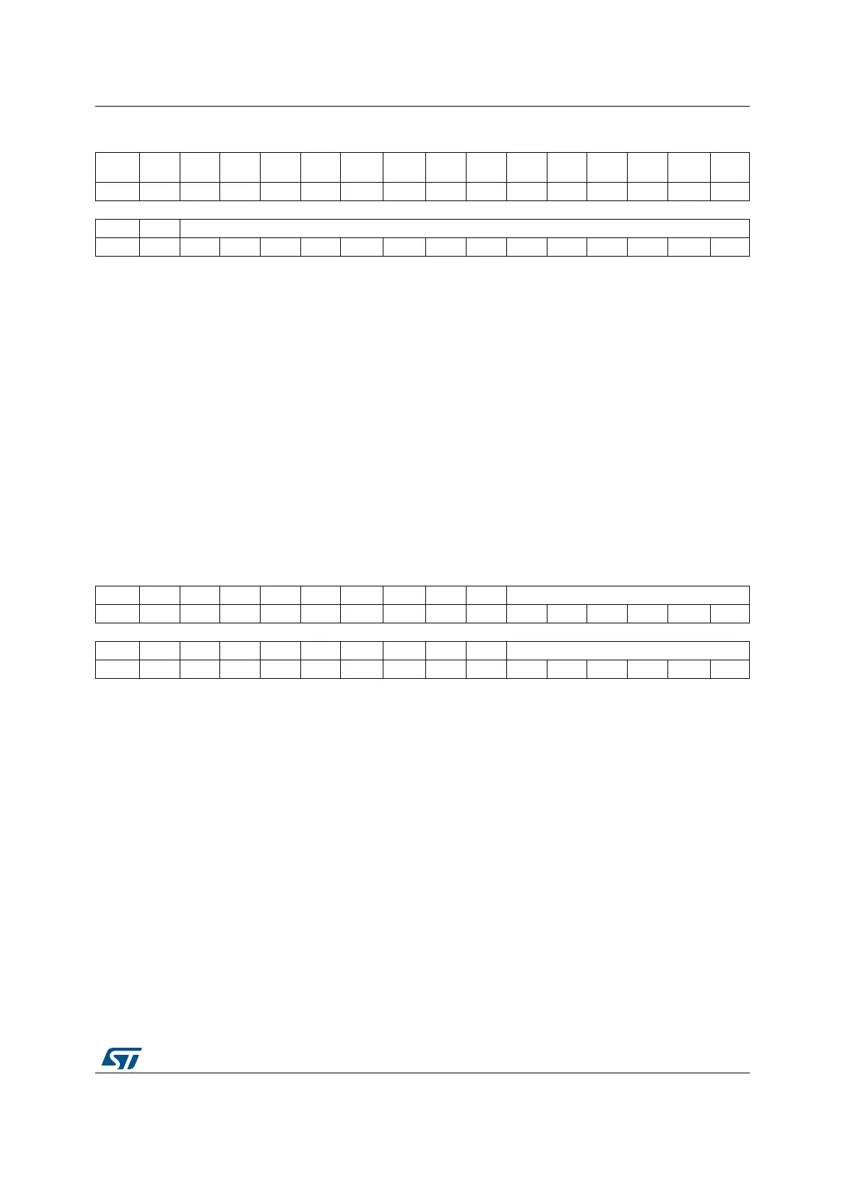
WRP1 Area A address option bytes
Flash memory address: 0x1FFF 7818
ST production value: 0xFF00 FFFF
31 30 29 28 27 26 25 24 23 22 21 20 19 18 17 16
PCROP
_RDP
Res. Res. Res. Res. Res. Res. Res. Res. Res. Res. Res. Res. Res. Res. Res.
rw
15 14 13 12 11 10 9 8 7 6 5 4 3 2 1 0
Res. Res. PCROP1_END[13:0]
rw rw rw rw rw rw rw rw rw rw rw rw rw rw
Bit 31 PCROP_RDP: PCROP area preserved when RDP level decreased
This bit is set only. It is reset after a full mass erase due to a change of RDP
from Level 1 to Level 0.
0: PCROP area is not erased when the RDP level is decreased from Level 1 to
Level 0.
1: PCROP area is erased when the RDP level is decreased from Level 1 to
Level 0 (full mass erase).
Bits 30:14 Reserved, must be kept at reset value.
Bits 13:0 PCROP1_END: Bank 1 PCROP area end offset
PCROP1_END contains the last double-word of the PCROP area.
31 30 29 28 27 26 25 24 23 22 21 20 19 18 17 16
Res. Res. Res. Res. Res. Res. Res. Res. Res. Res. WRP1A_END[5:0]
rw rw rw rw rw rw
15 14 13 12 11 10 9 8 7 6 5 4 3 2 1 0
Res. Res. Res. Res. Res. Res. Res. Res. Res. Res. WRP1A_STRT[5:0]
rw rw rw rw rw rw
Bits 31:22 Reserved, must be kept at reset value.
Bits 21:16 WRP1A_END: WRP first area “A” end offset
WRP1A_END contains the last page of WRP first area.
Bits 15:6 Reserved, must be kept at reset value.
Bits 5:0 WRP1A_STRT: WRP first area “A” start offset
WRP1A_STRT contains the first page of WRP first area.
 Loading...


