RM0440 Rev 4 379/2126
RM0440 System configuration controller (SYSCFG)
380
10.2.9 SYSCFG CCM SRAM write protection register (SYSCFG_SWPR)
Address offset: 0x20
System reset value: 0x0000 0000
10.2.10 SYSCFG CCM SRAM key register (SYSCFG_SKR)
Address offset: 0x24
System reset value: 0x0000 0000
Bit 0 CLL: Cortex
®
-M4 LOCKUP (Hardfault) output enable bit
This bit is set by software and cleared only by a system reset. It can be used to
enable and lock the connection of Cortex
®
-M4 with FPU LOCKUP (Hardfault)
output to TIM1/8/15/16/17/20 break input and hrtim_sys_flt input of HRTIM1.
0: Cortex
®
-M4 LOCKUP output disconnected from TIM1/8/15/16/17/20 break
input and hrtim_sys_flt input of HRTIM1.
1: Cortex
®
-M4 LOCKUP output connected to TIM1/8/15/16/17/20 break input
and hrtim_sys_flt input of HRTIM1.
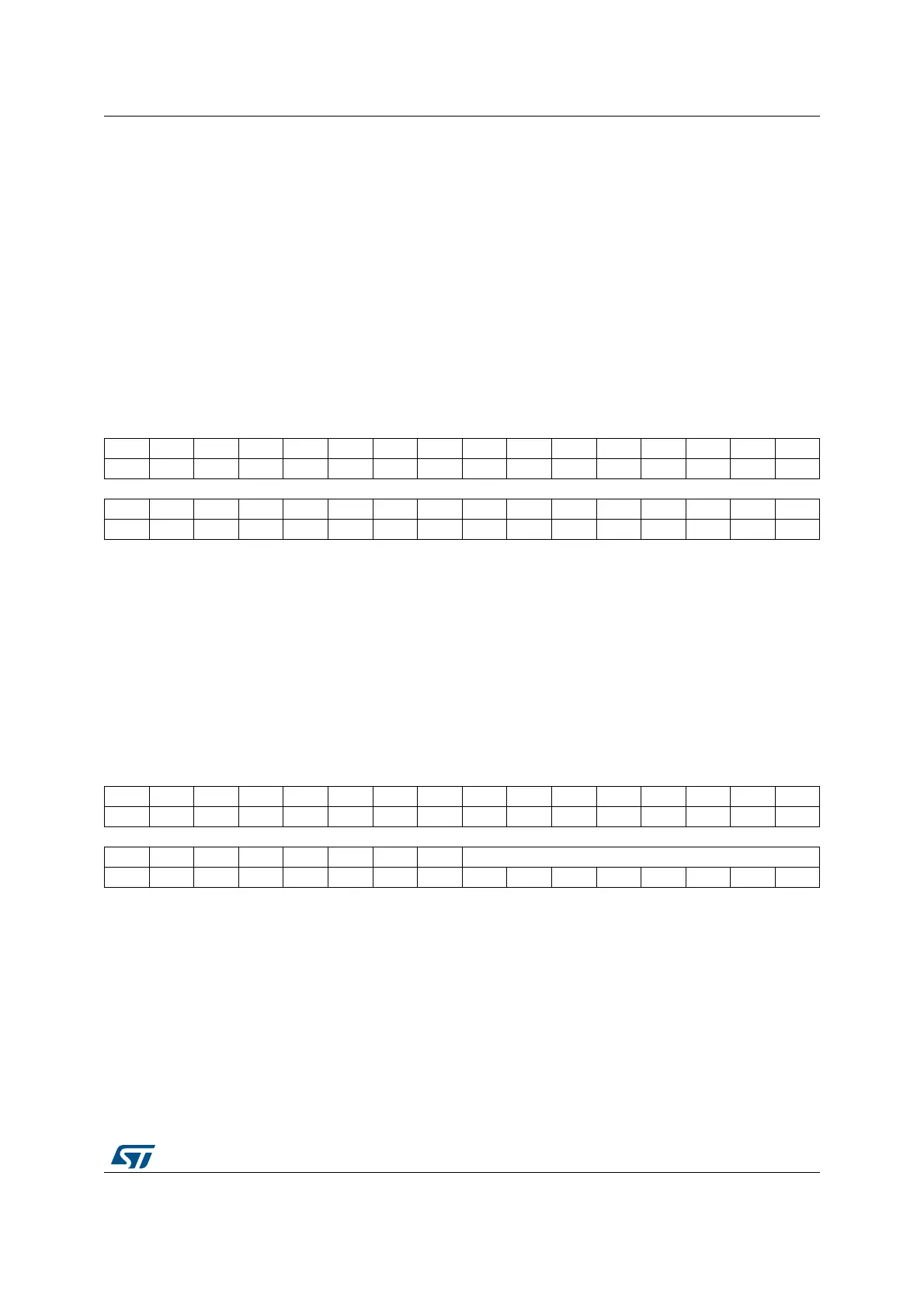
31 30 29 28 27 26 25 24 23 22 21 20 19 18 17 16
P31WP P30WP P29WP P28WP P27WP P26WP P25WP P24WP P23WP P22WP P21WP P20WP P19WP P18WP P17WP P16WP
rs rs rs rs rs rs rs rs rs rs rs rs rs rs rs rs
1514131211109876543210
P15WP P14WP P13WP P12WP P11WP P10WP P9WP P8WP P7WP P6WP P5WP P4WP P3WP P2WP P1WP P0WP
rs rs rs rs rs rs rs rs rs rs rs rs rs rs rs rs
Bits 31:0 PxWP (x = 0 to 31): CCM SRAM page x write protection
These bits are set by software and cleared only by a system reset.
0: Write protection of CCM SRAM page x is disabled.
1: Write protection of CCM SRAM page x is enabled.
31 30 29 28 27 26 25 24 23 22 21 20 19 18 17 16
Res Res Res Res Res Res Res Res Res Res Res Res Res Res Res Res
1514131211109876543210
Res Res Res Res Res Res Res Res KEY[7:0]
wwwwwwww
Bits 31:8 Reserved, must be kept at reset value
Bits 7:0 KEY[7:0]: CCM SRAM write protection key for software erase
The following steps are required to unlock the write protection of the CCMER bit
in the SYSCFG_SCSR register.
1. Write "0xCA” into Key[7:0]
2. Write "0x53” into Key[7:0]
Writing a wrong key reactivates the write protection.
 Loading...


