Debug support (DBG) RM0453
1314/1450 RM0453 Rev 5
38.3.2 DBG pins and internal signals
38.3.3 DBG interface control
Device debug access is controlled from the following parameters:
• User option RDP level, as described in Section 4.6.1: Readout protection (RDP)
• User option DDS, as described in Section 4: Embedded flash memory (FLASH)
• User option HDPAD (Hide protection access disable), as described in Section 4:
Embedded flash memory (FLASH)
• Flash register bit C2SWDBGEN as described in Section 4: Embedded flash memory
(FLASH)
Debug access control is independent from ESE.
Debug access to the CPUs is shown in the table below.
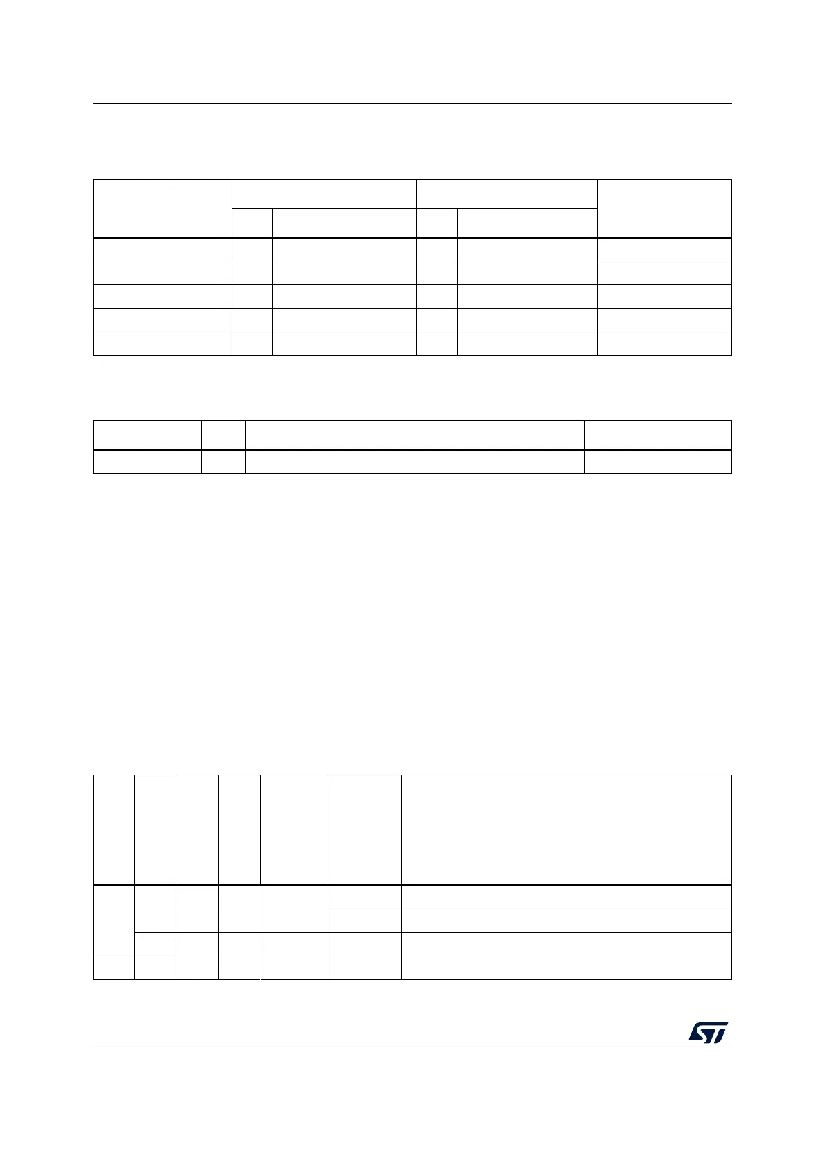
Table 260. JTAG/Serial-wire debug port pins
Pin name
JTAG debug port Serial-wire debug port
Pin assignment
Type Description Type Description
JTMS/SWDIO I JTAG test mode select IO Serial wire data in/out PA13
JTCK/SWCLK I JTAG test clock I Serial wire clock PA14
JTDI I JTAG test data input - - PA15
JTDO/TRACESWO
(1)
O JTAG test data output - - PB3
nJTRST I JTAG test reset - - PB4
1. Debug access port JTDO and Trace port TRACESWO are multiplexed on a single device GPIO pin.
Table 261. Single-wire trace port pins
Pin name Type Description Pin assignment
TRACESWO O Single wire trace asynchronous data out PB3
(1)
1. TRACESWO is multiplexed with JTDO. This means that single-wire trace is only available when using the Serial-wire
debug interface, and not when using JTAG.
Table 262. Debug access control overview
RDP
DDS
C2SWDBGEN
RSS boot
CPU1
debug
CPU2
debug
Comment
0 or 1
0
1
No Enabled
Enabled When HDPAD = 1, C2SWDBGEN is enabled from reset.
0 Disabled When HDPAD = 0, C2SWDBGEN is disabled from reset.
1 x No Enabled Disabled Cortex-M0+ debug is disabled by DDS.
2 x x x Disabled Disabled Debug is disabled by RDP level 2.