Power control (PWR) RM0453
270/1450 RM0453 Rev 5
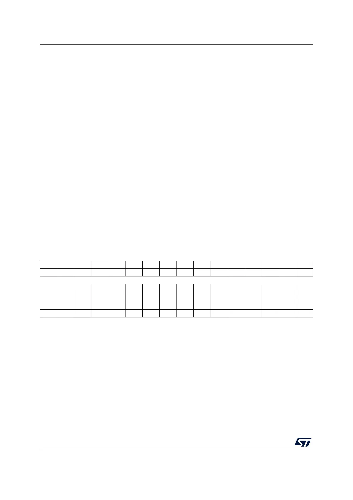
6.6.6 Power status register 2 (PWR_SR2)
This register is partially reset when exiting Standby/Shutdown modes.
Address offset: 0x014
Reset value: 0x0000 0000
Bit 11 WRFBUSYF: Radio busy wake-up flag
This bit is set when a wake-up event is detected on radio busy. It is cleared by writing ‘1’ in
the CWRFBUSYF bit of the PWR_SCR register.
Bits 10:9 Reserved, must be kept at reset value.
Bit 8 WPVDF: Wake-up PVD flag
This bit is set when a wake-up event is detected on PVD. It is cleared by writing ‘1’ in the
CWPVDF bit of the PWR_SCR register.
Bits 7:3 Reserved, must be kept at reset value.
Bit 2 WUF3: Wake-up flag 3
This bit is set when a wake-up event is detected on wake-up pin, WKUP3. It is cleared by
writing 1 in the CWUF3 bit of the PWR status clear register (PWR_SCR).
Bit 1 WUF2: Wake-up flag 2
This bit is set when a wake-up event is detected on wake-up pin, WKUP2. It is cleared by
writing 1 in the CWUF2 bit of the PWR status clear register (PWR_SCR).
Bit 0 WUF1: Wake-up flag 1
This bit is set when a wake-up event is detected on wake-up pin, WKUP1. It is cleared by
writing 1 in the CWUF1 bit of the PWR status clear register (PWR_SCR).
31 30 29 28 27 26 25 24 23 22 21 20 19 18 17 16
Res. Res. Res. Res. Res. Res. Res. Res. Res. Res. Res. Res. Res. Res. Res. Res.
1514131211109876543210
Res. PVMO3 Res. Res. PVDO VOSF
REGLPF
REGLPS
FLASHRDY
REGMRS
RFEOLF
LDORDY
SMPSRDY
RFBUSYMS
RFBUSYS
C2BOOTS
r rrrrrrrrrrrr
Bits 31:15 Reserved, must be kept at reset value.
Bit 14 PVMO3: Peripheral voltage monitoring output: V
DDA
versus 1.62 V
0: V
DDA
voltage above PVM3 threshold (around 1.62 V)
1: V
DDA
voltage below PVM3 threshold (around 1.62 V)
Note: PVMO3 is cleared when PVM3 is disabled (PVME3 = 0). After enabling PVM3, the
PVM3 output is valid after the PVM3 wake-up time.
Bits 13:12 Reserved, must be kept at reset value.
Bit 11 PVDO: Programmable voltage detector output
0: V
DD
or voltage level on PVD_IN above the selected PVD threshold
1: V
DD
or voltage level on PVD_IN below the selected PVD threshold