General-purpose timers (TIM16/TIM17) RM0453
910/1450 RM0453 Rev 5
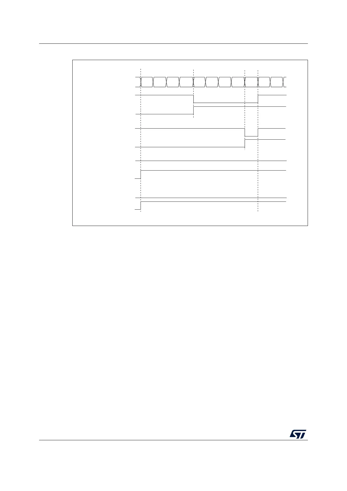
Figure 254. Edge-aligned PWM waveforms (ARR=8)
27.3.10 Complementary outputs and dead-time insertion
The TIM16/TIM17 general-purpose timers can output one complementary signal and
manage the switching-off and switching-on of the outputs.
This time is generally known as dead-time and it has to be adjusted depending on the
devices that are connected to the outputs and their characteristics (intrinsic delays of level-
shifters, delays due to power switches...)
The polarity of the outputs (main output OCx or complementary OCxN) can be selected
independently for each output. This is done by writing to the CCxP and CCxNP bits in the
TIMx_CCER register.
The complementary signals OCx and OCxN are activated by a combination of several
control bits: the CCxE and CCxNE bits in the TIMx_CCER register and the MOE, OISx,
OISxN, OSSI and OSSR bits in the TIMx_BDTR and TIMx_CR2 registers. Refer to
Table 187: Output control bits for complementary OCx and OCxN channels with break
feature (TIM16/17) on page 932 for more details. In particular, the dead-time is activated
when switching to the idle state (MOE falling down to 0).
Dead-time insertion is enabled by setting both CCxE and CCxNE bits, and the MOE bit if the
break circuit is present. There is one 10-bit dead-time generator for each channel. From a
reference waveform OCxREF, it generates 2 outputs OCx and OCxN. If OCx and OCxN are
active high:
• The OCx output signal is the same as the reference signal except for the rising edge,
which is delayed relative to the reference rising edge.
• The OCxN output signal is the opposite of the reference signal except for the rising
edge, which is delayed relative to the reference falling edge.
MS31093V1
Counter register
‘1’
0
12 3456 7801
OCXREF
CCxIF
OCXREF
CCxIF
OCXREF
CCxIF
OCXREF
CCxIF
CCRx=4
CCRx=8
CCRx>8
CCRx=0
‘0’