RM0453 Rev 5 229/1450
RM0453 Power control (PWR)
285
VREF+ pin is not available on all packages. When not available, this pin is internally
bonded to VDDA. When VREF+ is double-bonded with VDDA in a package, the
internal voltage reference buffer is not available and must be kept disabled (refer to the
datasheet for pinout descriptions).
During power up and power down, the following power sequence is required:
1. When V
DD
< 1 V other power supplies (V
DDA
) must remain below V
DD
+ 300 mV.
During power down, V
DD
can temporarily become lower then other supplies only if the
energy provided to the device remains below 1 mJ. This allows external decoupling
capacitors to be discharged with different time constants during this transient phase.
2. When V
DD
> 1 V, all other power supplies (V
DDA
) become independent.
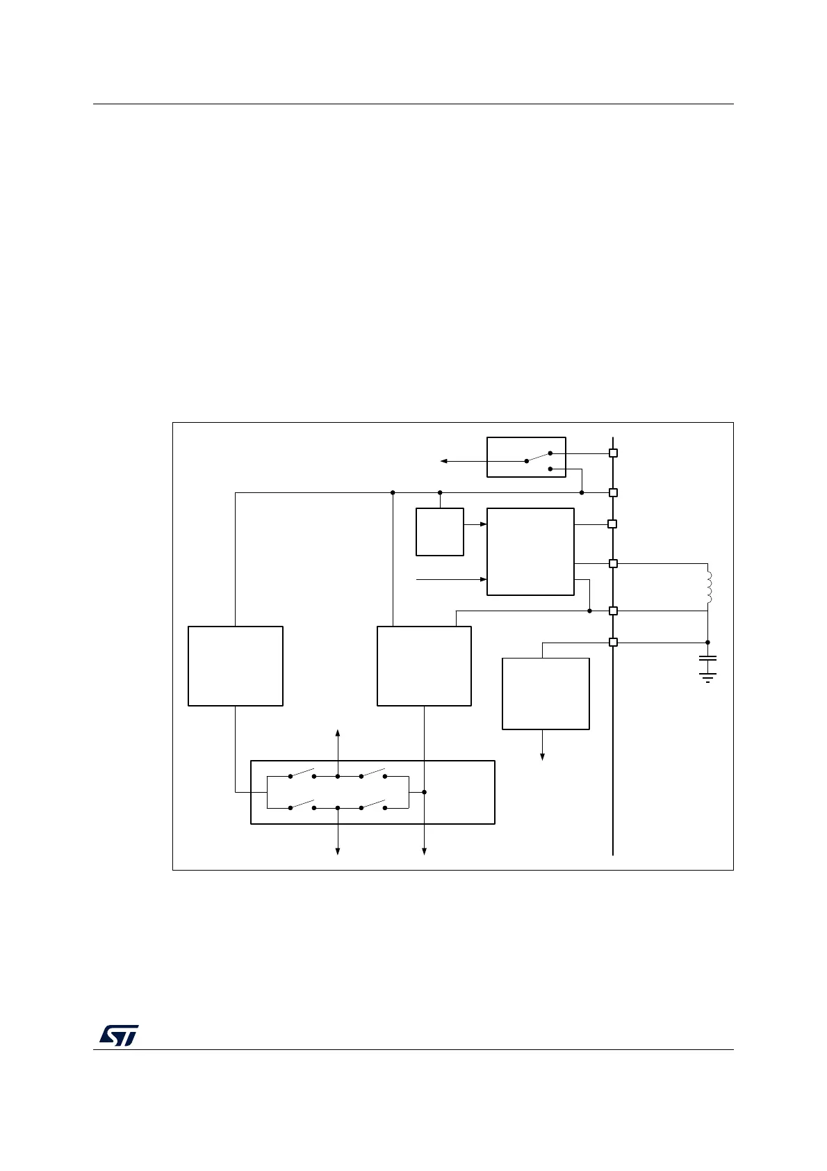
An embedded linear voltage regulator is used to supply the internal digital power V
CORE
.
V
CORE
is the power supply for digital peripherals, SRAM1 and SRAM2. The flash memory is
supplied by V
CORE
and V
DD
. V
CORE
is split in two parts: V
DDO
part and an interruptible part
V
DDI
.
Figure 18. Power supply overview
MSv50973V2
LDO/SMPS
MR
V
DD
V
LXSMPS
V
FBSMPS
V
BKP
V
DDO
V
DDI
V
BAT
V
RF
V
MAIN
V
LP
V
SW
POR
mode
FW mode
en
RFLDO
V
DDSMPS
V
DDRF1V5
LPR