RM0453 Rev 5 619/1450
RM0453 Voltage reference buffer (VREFBUF)
619
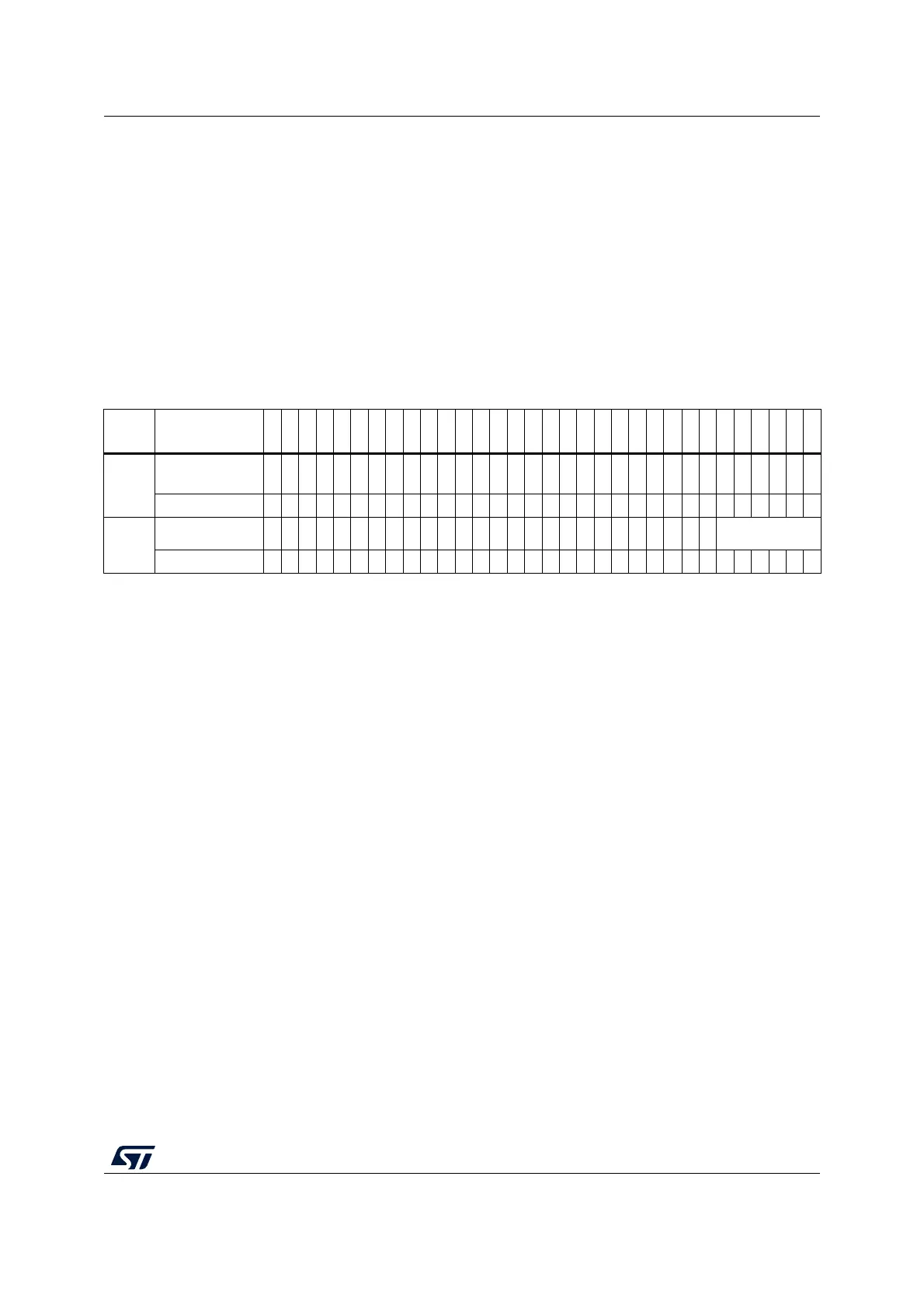
20.3.3 VREFBUF register map
The following table gives the VREFBUF register map and the reset values.
Refer to Section 2.6 for the register boundary addresses.
Bits 31:6 Reserved, must be kept at reset value.
Bits 5:0 TRIM[5:0]: Trimming code
These bits are automatically initialized after reset with the trimming value stored in the flash
memory during the production test. Writing into these bits allows the tuning of the internal
reference buffer voltage.
Note: If the user application performs the trimming, the trimming code must start from 000000
to 111111 in ascending order.
Table 121. VREFBUF register map and reset values
Offset Register name
31
30
29
28
27
26
25
24
23
22
21
20
19
18
17
16
15
14
13
12
11
10
9
8
7
6
5
4
3
2
1
0
0x00
VREFBUF_CSR
Res.
Res.
Res.
Res.
Res.
Res.
Res.
Res.
Res.
Res.
Res.
Res.
Res.
Res.
Res.
Res.
Res.
Res.
Res.
Res.
Res.
Res.
Res.
Res.
Res.
Res.
Res.
Res.
VRR
VRS
HIZ
ENVR
Reset value 0010
0x04
VREFBUF_CCR
Res.
Res.
Res.
Res.
Res.
Res.
Res.
Res.
Res.
Res.
Res.
Res.
Res.
Res.
Res.
Res.
Res.
Res.
Res.
Res.
Res.
Res.
Res.
Res.
Res.
Res.
TRIM[5:0]
Reset value xxxxxx